ChipApex | Global Electronic Components Supplier

SEARCH
Search Product
Search Post
— IC芯片 | 连接器 | 传感器 | 被动器件 —
Search productSearch post
— IC芯片 | 连接器 | 传感器 | 被动器件 —
Consult the customer manager about the wholesale price.
consultation hotline:86-132-6715-2157
email:[email protected]
Contact the product manager for consultation. One-stop consultation is available.
Do you want a lower wholesale price? Please send us your inquiry and we will reply immediately.
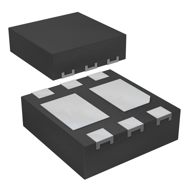
The PMCPB5530XAX is a complementary N/P-channel enhancement mode Field-Effect Transistor utilizing Trench MOSFET technology in a DFN2020-6 (SOT1118) package. The N-channel device supports a drain-source voltage of 20 V and continuous current up to 4.5 A, with a typical on-resistance of 26 mΩ. The P-channel counterpart handles -20 V and -3.6 A, featuring a typical on-resistance of 50 mΩ. Both transistors operate within a junction temperature range of -55 °C to +150 °C.
Verify the specific suffix 'AX' against the manufacturer's official ordering information to confirm reel packaging specifications. Ensure design compliance with AEC-Q101 automotive qualification requirements if deploying in vehicle electronics. Confirm thermal management aligns with the specified junction-to-ambient resistance values for the target PCB footprint.
Select this component for designs requiring a compact dual-transistor solution with high thermal efficiency. The low gate charge and fast switching characteristics make it suitable for high-frequency power conversion. Evaluate the on-resistance at the intended operating gate voltage to ensure adequate drive capability and minimize conduction losses in the final application.
This part belongs to Nexperia's portfolio of small-signal and logic level MOSFETs designed for space-constrained surface-mount applications. It integrates both N-channel and P-channel devices into a single leadless package, reducing board space compared to discrete components while maintaining robust performance for general-purpose switching tasks.
PMCPB5530XA
The maximum peak drain current for the N-channel transistor (TR1) is 48 A under single-pulse conditions with a pulse width less than or equal to 10 µs.
Yes, the product has been qualified in accordance with the Automotive Electronics Council standard Q101, making it suitable for use in automotive applications.
The thermal resistance from junction to solder point (Rth(j-sp)) is typically 10 K/W per transistor and 11 K/W per device when mounted on an FR4 PCB.
 PMCPB5530XAX

The activity of extra discounts on wholesale prices is in full swing…
Please fill in your contact information and we will send you the latest wholesale price list.