ChipApex | Global Electronic Components Supplier

SEARCH
Search Product
Search Post
— IC芯片 | 连接器 | 传感器 | 被动器件 —
Search productSearch post
— IC芯片 | 连接器 | 传感器 | 被动器件 —
Consult the customer manager about the wholesale price.
consultation hotline:86-132-6715-2157
email:[email protected]
Contact the product manager for consultation. One-stop consultation is available.
Do you want a lower wholesale price? Please send us your inquiry and we will reply immediately.
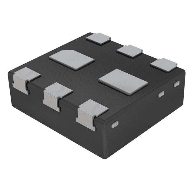
The PMCXB290UE is a complementary N/P-channel enhancement mode Field-Effect Transistor utilizing Trench MOSFET technology in a DFN1010B-6 (SOT1216) package. The N-channel device features a 20 V drain-source voltage and 930 mA continuous drain current with a typical on-resistance of 270 mΩ at VGS=4.5 V. The P-channel counterpart supports -20 V and -570 mA, exhibiting a typical on-resistance of 590 mΩ under identical gate drive conditions. Both channels operate within a junction temperature range of -55 °C to +150 °C.
Verify the specific ordering suffix against the manufacturer's official documentation to ensure correct packaging and tape-and-reel specifications. Confirm that the component status remains active or production-ready before finalizing procurement plans. Cross-reference the datasheet revision date to ensure compliance with the latest electrical characteristics and marking codes provided by Nexperia.
Select this component when a compact dual-transistor solution is required for low-voltage switching applications. The DFN1010B-6 package offers thermal efficiency through its exposed pad design. Ensure the application gate drive voltage aligns with the specified RDSon test conditions to achieve optimal conduction performance. Verify PCB footprint compatibility with the SOT1216 outline dimensions during the layout phase.
This part belongs to Nexperia's portfolio of small-signal MOSFETs designed for portable electronics. It integrates both N-channel and P-channel devices into a single leadless package, reducing board space compared to discrete solutions. The technology leverages advanced trench structures to minimize on-state resistance while maintaining high switching frequencies suitable for modern power management systems.
Direct pin-to-pin replacements require matching the DFN1010B-6 package and complementary channel configuration. Verify that substitute components meet the 20 V breakdown voltage and similar on-resistance thresholds. Check for equivalent ESD protection levels and thermal resistance characteristics to ensure reliable operation in the existing design.
The absolute maximum gate-source voltage is rated from -8 V to +8 V.
The drain-source on-state resistance increases as the junction temperature rises, with specific values provided for 25 °C and 150 °C in the characteristics table.
No, unless explicitly stated otherwise in the data sheet, this product is not automotive qualified and should not be used in life-critical or safety-critical systems.
 PMCXB290UEZ

The activity of extra discounts on wholesale prices is in full swing…
Please fill in your contact information and we will send you the latest wholesale price list.