ChipApex | Global Electronic Components Supplier

SEARCH
Search Product
Search Post
— IC芯片 | 连接器 | 传感器 | 被动器件 —
Search productSearch post
— IC芯片 | 连接器 | 传感器 | 被动器件 —
Consult the customer manager about the wholesale price.
consultation hotline:86-132-6715-2157
email:[email protected]
Contact the product manager for consultation. One-stop consultation is available.
Do you want a lower wholesale price? Please send us your inquiry and we will reply immediately.
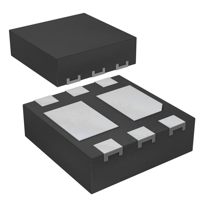
The PMDPB30XNA is a dual N-channel enhancement mode Field-Effect Transistor utilizing Trench MOSFET technology. It features a DFN2020-6 (SOT1118) leadless package with dimensions of 2 x 2 x 0.65 mm. Key electrical parameters include a drain-source voltage of 20 V, a continuous drain current of 4.5 A at 25 °C, and a typical on-state resistance of 26 mΩ at VGS = 4.5 V. The device operates within a junction temperature range of -55 °C to +150 °C.
Verify the specific ordering suffix against the manufacturer's official documentation to confirm packaging type and reel specifications. Confirm that the component meets the required AEC-Q101 qualification status if intended for automotive use. Ensure the design accounts for the thermal characteristics defined in the datasheet for the selected PCB footprint.
Select this component for designs requiring compact dual N-channel switching solutions with high thermal efficiency. The low on-state resistance supports efficient power management in portable devices. Verify that the gate drive voltage aligns with the specified threshold and on-state resistance conditions for optimal performance.
This part belongs to Nexperia's portfolio of small signal and logic MOSFETs designed for space-constrained applications. The DFN2020-6 package is part of the HUSON family, offering enhanced thermal performance compared to traditional leaded packages while maintaining a minimal footprint suitable for dense PCB layouts.
PMDPB30XNAX
The maximum drain-source voltage (VDS) is rated at 20 V.
Yes, the PMDPB30XNA is qualified in accordance with the AEC-Q101 standard.
The typical total gate charge (QG(tot)) is 6.6 nC under standard test conditions.
 PMDPB30XNAX

The activity of extra discounts on wholesale prices is in full swing…
Please fill in your contact information and we will send you the latest wholesale price list.