ChipApex | Global Electronic Components Supplier

SEARCH
Search Product
Search Post
— IC芯片 | 连接器 | 传感器 | 被动器件 —
Search productSearch post
— IC芯片 | 连接器 | 传感器 | 被动器件 —
Consult the customer manager about the wholesale price.
consultation hotline:86-132-6715-2157
email:[email protected]
Contact the product manager for consultation. One-stop consultation is available.
Do you want a lower wholesale price? Please send us your inquiry and we will reply immediately.
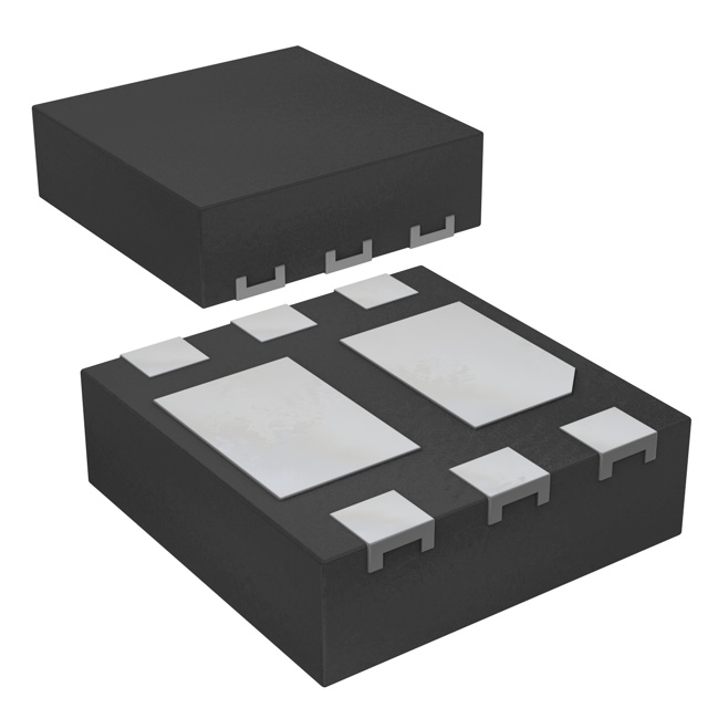
The PMDPB80XP is a dual P-channel enhancement mode Field-Effect Transistor utilizing Trench MOSFET technology. It is housed in an ultra-thin DFN2020-6 (SOT1118) package measuring 2 x 2 x 0.65 mm. The device supports a drain-source voltage of 20 V and a continuous drain current of 3.7 A at 25 °C. Key electrical parameters include a maximum RDSon of 102 mΩ at VGS = -4.5 V, a gate-source threshold voltage ranging from -0.4 V to -1 V, and a total gate charge of 8.6 nC.
Verify the component marking code '1U' against the datasheet to confirm authenticity. Ensure the ordering suffix matches the specified package variant. Confirm that the application environment remains within the stated junction temperature limits and absolute maximum ratings defined in the official Nexperia documentation.
Select this component when space constraints require an ultra-thin footprint with high thermal efficiency. The low RDSon rating supports efficient power switching in portable electronics. Verify that the required gate drive voltage aligns with the specified threshold characteristics for optimal performance.
This dual FET integrates two independent P-channel transistors into a single compact package. The design reduces PCB area compared to discrete solutions. The exposed drain pad facilitates heat dissipation, supporting reliable operation in thermally constrained environments typical of modern portable electronic devices.
No public confirmed substitute part numbers are documented in the provided source material.
The maximum drain-source voltage (VDS) is rated at 20 V.
The DFN2020-6 package features an exposed drain pad designed for excellent thermal conduction to the PCB.
The typical gate-source threshold voltage (VGSth) is -0.6 V under standard test conditions.
 PMDPB80XP,115

The activity of extra discounts on wholesale prices is in full swing…
Please fill in your contact information and we will send you the latest wholesale price list.