ChipApex | Global Electronic Components Supplier

SEARCH
Search Product
Search Post
— IC芯片 | 连接器 | 传感器 | 被动器件 —
Search productSearch post
— IC芯片 | 连接器 | 传感器 | 被动器件 —
Consult the customer manager about the wholesale price.
consultation hotline:86-132-6715-2157
email:[email protected]
Contact the product manager for consultation. One-stop consultation is available.
Do you want a lower wholesale price? Please send us your inquiry and we will reply immediately.
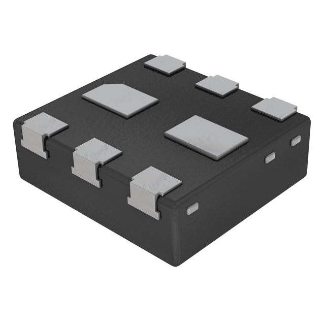
The PMDXB1200UPE is a dual P-channel enhancement mode Field-Effect Transistor utilizing Trench MOSFET technology. It is housed in a leadless ultra small DFN1010B-6 (SOT1216) plastic package measuring 1.1 x 1.0 x 0.37 mm. The device features a drain-source voltage of -30 V and a gate-source voltage range of -8 to 8 V. Each transistor supports a continuous drain current of -410 mA at 25 °C, with a peak current of -1.7 A. The typical on-state resistance is 1.2 Ω at VGS = -4.5 V. Total power dissipation reaches 285 mW in free air.
Verify the specific ordering suffix against official Nexperia documentation to confirm packaging format and tape-and-reel specifications. Confirm that the component status remains active production rather than obsolete or end-of-life. Ensure the procurement channel provides valid traceability data consistent with Nexperia quality standards.
Select this component when space constraints require dual P-channel functionality in an ultra-thin profile. The low threshold voltage makes it suitable for applications driven by standard logic levels. Evaluate thermal performance based on the specified junction-to-ambient resistance values for your specific PCB copper area and mounting conditions.
This device belongs to Nexperia's portfolio of TrenchMOS FETs designed for general-purpose power switching. It utilizes advanced trench technology to achieve low on-resistance within a miniature leadless package. The dual configuration allows for cost-effective implementation of bridge or high-side switching topologies in portable and industrial electronics.
Direct replacements must match the dual P-channel topology, -30 V rating, and SOT1216 package dimensions. Verify equivalent RDSon characteristics and pinout compatibility before substitution.
The maximum junction temperature is 150 °C.
Yes, the device includes ElectroStatic Discharge protection rated above 2 kV HBM.
It uses a leadless ultra small DFN1010B-6 plastic package, also known as SOT1216.
 PMDXB1200UPEZ

The activity of extra discounts on wholesale prices is in full swing…
Please fill in your contact information and we will send you the latest wholesale price list.