ChipApex | Global Electronic Components Supplier

SEARCH
Search Product
Search Post
— IC芯片 | 连接器 | 传感器 | 被动器件 —
Search productSearch post
— IC芯片 | 连接器 | 传感器 | 被动器件 —
Consult the customer manager about the wholesale price.
consultation hotline:86-132-6715-2157
email:[email protected]
Contact the product manager for consultation. One-stop consultation is available.
Do you want a lower wholesale price? Please send us your inquiry and we will reply immediately.
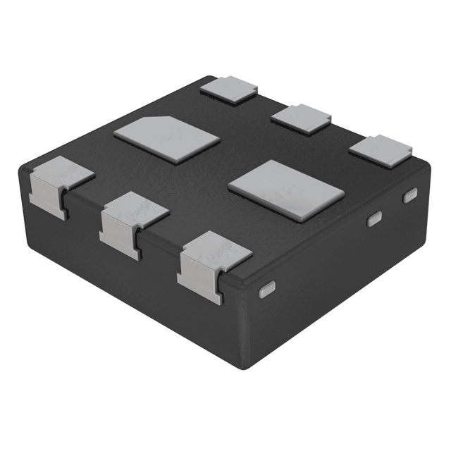
The PMDXB950UPELZ is a dual P-channel enhancement mode Field-Effect Transistor utilizing Trench MOSFET technology. It is housed in a leadless DFN1010B-6 (SOT1216) package measuring 1.1 × 1.0 × 0.37 mm. Key electrical parameters include a drain-source voltage of -20 V, a continuous drain current of -500 mA at 25 °C, and a typical drain-source on-state resistance of 1.02 Ω. The device features an exposed drain pad for thermal management and offers ESD protection exceeding 1 kV HBM.
Verify the specific ordering suffix against the manufacturer's official documentation to ensure correct packaging and tape-and-reel specifications. Confirm that the component meets all required environmental and reliability standards for the intended application before finalizing procurement orders.
Select this component for applications requiring compact dual P-channel switching with low on-resistance. Ensure the design accommodates the thermal requirements associated with the DFN1010B-6 package and utilizes the exposed drain pad for effective heat dissipation.
This part belongs to Nexperia's Trench MOSFET series, designed for space-constrained surface-mount applications. The DFN1010B-6 package is optimized for thermal performance and mechanical stability in small outline form factors.
Consult official Nexperia substitution guides for verified alternatives. Do not assume pin-compatible replacements without verifying electrical parameters and package dimensions.
The maximum gate-source voltage is rated at 8 V and -8 V.
Yes, the device provides ElectroStatic Discharge (ESD) protection greater than 1 kV HBM.
The typical total gate charge (QG(tot)) is 1.19 nC under standard test conditions.
 PMDXB950UPELZ

The activity of extra discounts on wholesale prices is in full swing…
Please fill in your contact information and we will send you the latest wholesale price list.