 ChipApex | Global Electronic Components Supplier

SEARCH
Search Product
Search Post
— IC芯片 | 连接器 | 传感器 | 被动器件 —
Search productSearch post
— IC芯片 | 连接器 | 传感器 | 被动器件 —
Consult the customer manager about the wholesale price.
consultation hotline:86-132-6715-2157
email:[email protected]
Contact the product manager for consultation. One-stop consultation is available.
Do you want a lower wholesale price? Please send us your inquiry and we will reply immediately.
The PMGD175XN is a dual N-channel enhancement mode Field-Effect Transistor utilizing Trench MOSFET technology in a SOT363 (TSSOP6) surface-mounted package. It features a drain-source voltage of 30 V and a gate-source voltage range of -12 V to 12 V. The continuous drain current is rated at 1 A per transistor under specific thermal conditions, with a maximum total power dissipation of 390 mW for the device. Key electrical parameters include a typical drain-source on-state resistance of 225 mΩ at 4.5 V gate drive and 1 A drain current. The component supports a junction temperature range from -55 °C to 150 °C.
Verify the manufacturer origin, as the product was originally an NXP Standard Product before becoming part of Nexperia. Confirm the specific ordering suffix matches the required packaging format. Ensure the datasheet version aligns with current production specifications. Check for automotive qualification status if intended for vehicle applications, as standard versions may lack specific automotive certifications.
Select this component for applications requiring dual N-channel switching in a minimal footprint. Evaluate the thermal resistance characteristics against the expected PCB copper area and ambient temperature. Ensure the gate drive voltage meets the minimum threshold for optimal RDS(on) performance. Consider the peak drain current limits for transient loads exceeding the continuous rating.
This device belongs to the family of dual N-channel Trench MOSFETs designed for low-voltage switching applications. It shares architectural similarities with other small-signal MOSFETs but distinguishes itself through the integration of two channels in the SOT363 package. The technology leverages trench structures to reduce on-resistance while maintaining high switching speeds suitable for modern electronic designs.
PMGD175XNE is a verified equivalent part number representing the same device with potential packaging variations.
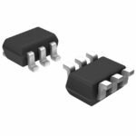 PMGD175XN,115

The activity of extra discounts on wholesale prices is in full swing…
Please fill in your contact information and we will send you the latest wholesale price list.





