ChipApex | Global Electronic Components Supplier

SEARCH
Search Product
Search Post
— IC芯片 | 连接器 | 传感器 | 被动器件 —
Search productSearch post
— IC芯片 | 连接器 | 传感器 | 被动器件 —
Consult the customer manager about the wholesale price.
consultation hotline:86-132-6715-2157
email:[email protected]
Contact the product manager for consultation. One-stop consultation is available.
Do you want a lower wholesale price? Please send us your inquiry and we will reply immediately.
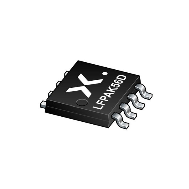
The Nexperia PSMN8R5-40HSX is a dual standard level N-channel MOSFET housed in an LFPAK56D (Dual Power-SO8) package utilizing TrenchMOS technology. It features a drain-source voltage of 40 V and a continuous drain current of 30 A at a mounting base temperature of 25 °C. The typical drain-source on-state resistance is 8.5 mΩ at VGS = 10 V and ID = 15 A, rising to 16.7 mΩ maximum at 175 °C. Total power dissipation reaches 53 W under specified conditions. The device supports junction temperatures from -55 °C to 175 °C and includes repetitive avalanche rating capabilities.
Verify the specific ordering suffix against the manufacturer's official documentation to confirm exact packaging and reel specifications. Confirm that the LFPAK56D footprint matches your PCB design guidelines. Ensure thermal management strategies account for the 53 W total power dissipation limit at 25 °C mounting base temperature. Check for any recent product status updates or obsolescence notices directly from Nexperia before finalizing procurement plans.
Select this component when a dual N-channel configuration is required in a space-constrained Dual Power-SO8 form factor. The 8.5 mΩ on-state resistance offers low conduction losses for standard level gate drive applications. Consider the 175 °C qualification for thermally demanding environments. Verify that the 40 V breakdown voltage aligns with your system's maximum operating voltages and transient requirements.
This device belongs to Nexperia's standard level N-channel MOSFET portfolio, leveraging TrenchMOS technology for optimized performance. It is designed as a dual solution to save board space compared to using two separate single MOSFETs. The LFPAK56D package provides enhanced thermal performance through its exposed pad and copper-clip construction, suitable for high-efficiency power switching applications.
Consult Nexperia's official cross-reference tools for verified substitutes. Single-channel equivalents like the PSMN8R5-40YS may require two units to match functionality. Ensure any replacement maintains the LFPAK56D footprint or requires PCB redesign. Verify that alternative parts meet the same 175 °C qualification and avalanche ruggedness standards.
The maximum non-repetitive drain-source avalanche energy is 84 mJ, tested at ID = 30 A, Vsup ≤ 40 V, VGS = 10 V, and initial junction temperature of 25 °C.
At VGS = 10 V and ID = 15 A, the typical RDS(on) is 8.5 mΩ at 25 °C and increases to a maximum of 16.7 mΩ at 175 °C junction temperature.
No, unless explicitly stated otherwise in the data sheet, this product is not suitable for automotive use and is not qualified or tested according to automotive testing requirements.
 PSMN8R5-40HSX

The activity of extra discounts on wholesale prices is in full swing…
Please fill in your contact information and we will send you the latest wholesale price list.