ChipApex | Global Electronic Components Supplier
SEARCH
Search Product
Search Post
— IC芯片 | 连接器 | 传感器 | 被动器件 —
Search productSearch post
— IC芯片 | 连接器 | 传感器 | 被动器件 —
Consult the customer manager about the wholesale price.
consultation hotline:86-132-6715-2157
email:[email protected]
Contact the product manager for consultation. One-stop consultation is available.
Do you want a lower wholesale price? Please send us your inquiry and we will reply immediately.
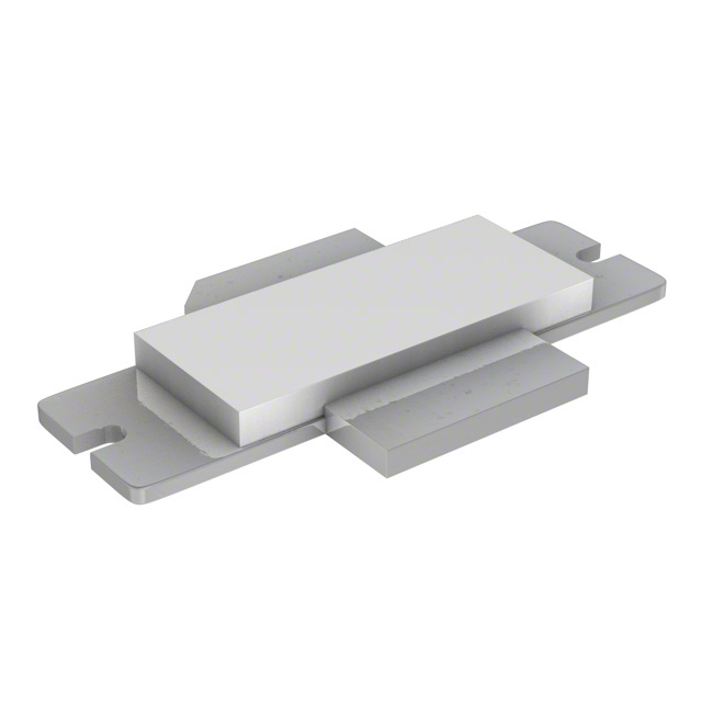
The PTFA181001E V4 T500 is a 100-watt LDMOS FET designed for EDGE and WCDMA power amplifier applications in the DCS band. It operates within the 1805–1880 MHz frequency range with integrated input and output matching. The device utilizes Infineon's advanced LDMOS process to provide excellent thermal performance and superior reliability. Key electrical characteristics include a drain-source breakdown voltage of 65 V, a typical linear gain of 16.5 dB, and a drain efficiency of 36% under EDGE modulation conditions at 28 V.
Verify the specific package variant (H-36248-2 for slotted flange) against the design requirements. Confirm that the V4 revision matches the intended footprint and pinout configuration. Ensure handling precautions are strictly followed due to the device being an electrostatic discharge sensitive component. Cross-reference the ordering information to validate the exact marking and version details before finalizing procurement.
Select this component for high-power RF applications requiring broadband internal matching and robust thermal management. The device supports both EDGE and WCDMA signals with verified linearity and efficiency metrics. Consider the specific package type based on the available mounting space and cooling infrastructure. Evaluate the 65 V drain-source breakdown voltage to ensure compatibility with the system's 28 V operating supply.
This part belongs to Infineon's portfolio of thermally-enhanced high-power RF LDMOS FETs. Manufactured using advanced LDMOS technology, these devices are engineered for demanding wireless communication environments. The product line emphasizes reliability and ease of integration through built-in matching networks and specialized packaging solutions tailored for high-frequency power amplification.
The datasheet does not list public confirmed substitute part numbers. Verify compatibility with existing designs by comparing package dimensions, pin configurations, and electrical parameters against alternative components.


 PTFA181001E V4 T500
The activity of extra discounts on wholesale prices is in full swing…
Please fill in your contact information and we will send you the latest wholesale price list.