ChipApex | Global Electronic Components Supplier

SEARCH
Search Product
Search Post
— IC芯片 | 连接器 | 传感器 | 被动器件 —
Search productSearch post
— IC芯片 | 连接器 | 传感器 | 被动器件 —
Consult the customer manager about the wholesale price.
consultation hotline:86-132-6715-2157
email:[email protected]
Contact the product manager for consultation. One-stop consultation is available.
Do you want a lower wholesale price? Please send us your inquiry and we will reply immediately.
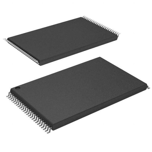
S29JL032J60TFI413 is listed in the Memory IC range at ChipApex. The manufacturer field lists Infineon Technologies. Its product description is IC FLASH 32MBIT PARALLEL 48TSOP. Review the specifications below when checking this part for your BOM.
The Infineon S29JL032J60TFI413 is a 32-Mb (4M x 8-bit / 2M x 16-bit) NOR flash memory device operating on a single 3.0 V supply. It features simultaneous read/write operations with zero latency, allowing data access from one bank while programming or erasing occurs in another. The device supports top boot sector configuration with two banks of 16 Mb each. It offers a maximum access time of 60 ns and is housed in a 48-pin TSOP package. Designed for industrial applications, it operates within a temperature range of -40°C to +85°C.
Verify the specific ordering suffix '413' against official Infineon documentation to confirm the exact bank organization and boot sector configuration. Ensure the voltage supply matches the 3.0 V requirement and that the package type aligns with the 48-pin TSOP specification. Confirm industrial temperature grade compliance if operating outside standard commercial ranges.
Select this component when simultaneous read/write performance is critical for system responsiveness. The 60 ns access speed suits high-performance embedded applications. Consider the 48-pin TSOP package for surface-mount assembly constraints. Verify that the 3.0 V single-supply operation fits the target system's power budget.
The S29JL032J series belongs to Infineon's 3-Volt-only, 32-Mb Simultaneous Read/Write Flash Memory family. Originally developed by Cypress Semiconductor, these devices are manufactured using 0.11 µm process technology. The series provides flexible bank architectures and robust data retention characteristics suitable for demanding embedded environments.
S29GL064S70TFI040 is listed as a manufacturer-recommended substitute for similar S29JL032J variants. Verify pinout and command set compatibility before substitution.
The WP#/ACC pin serves dual functions: it acts as a hardware write protect input to secure boot sectors and can accept VHH to enable accelerated programming modes.
The device supports sector erase, chip erase, and erase suspend/resume operations, allowing users to pause erasure to read or program other sectors.
Explore related parts through Memory, Integrated Circuits (ICs), all product categories, ChipApex homepage.
 S29JL032J60TFI413
S29JL032J60TFI413 is listed in the Memory IC range at ChipApex. The manufacturer field lists Infineon Technologies. Its product description is IC FLASH 32MBIT PARALLEL…
Read More
S29JL032J60TFI413 is listed in the Memory IC range at ChipApex. The manufacturer field lists Infineon Technologies. Its product description is IC FLASH 32MBIT PARALLEL…
Read More
S29JL032J60TFI413 is listed in the Memory IC range at ChipApex. The manufacturer field lists Infineon Technologies. Its product description is IC FLASH 32MBIT PARALLEL…
Read More
S29JL032J60TFI413 is listed in the Memory IC range at ChipApex. The manufacturer field lists Infineon Technologies. Its product description is IC FLASH 32MBIT PARALLEL…
Read More
S29JL032J60TFI413 is listed in the Memory IC range at ChipApex. The manufacturer field lists Infineon Technologies. Its product description is IC FLASH 32MBIT PARALLEL…
Read More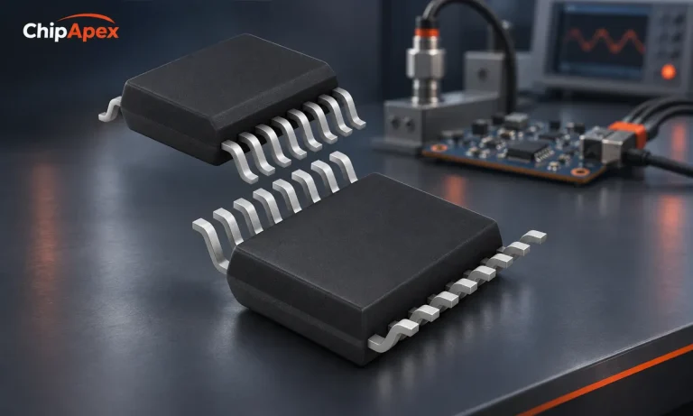
Choose an ADC converter by resolution, sample rate, noise and input design. Review practical tradeoffs and prepare component requirements for ChipApex.
Read More
S29JL032J60TFI413 is listed in the Memory IC range at ChipApex. The manufacturer field lists Infineon Technologies. Its product description is IC FLASH 32MBIT PARALLEL…
Read More
S29JL032J60TFI413 is listed in the Memory IC range at ChipApex. The manufacturer field lists Infineon Technologies. Its product description is IC FLASH 32MBIT PARALLEL…
Read More
S29JL032J60TFI413 is listed in the Memory IC range at ChipApex. The manufacturer field lists Infineon Technologies. Its product description is IC FLASH 32MBIT PARALLEL…
Read More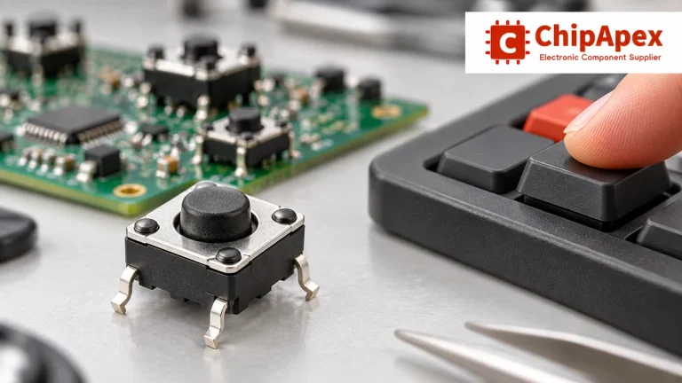
Understand tactile switches, PCB and keyboard differences, four-pin wiring, debounce, force, travel and replacement checks for reliable control inputs.
Read More
S29JL032J60TFI413 is listed in the Memory IC range at ChipApex. The manufacturer field lists Infineon Technologies. Its product description is IC FLASH 32MBIT PARALLEL…
Read More
S29JL032J60TFI413 is listed in the Memory IC range at ChipApex. The manufacturer field lists Infineon Technologies. Its product description is IC FLASH 32MBIT PARALLEL…
Read More
The activity of extra discounts on wholesale prices is in full swing…
Please fill in your contact information and we will send you the latest wholesale price list.