 ChipApex | Global Electronic Components Supplier
SEARCH
Search Product
Search Post
— IC芯片 | 连接器 | 传感器 | 被动器件 —
Search productSearch post
— IC芯片 | 连接器 | 传感器 | 被动器件 —
Consult the customer manager about the wholesale price.
consultation hotline:86-132-6715-2157
email:[email protected]
Contact the product manager for consultation. One-stop consultation is available.
Do you want a lower wholesale price? Please send us your inquiry and we will reply immediately.
The SH8M70TB1 is a silicon N-channel and P-channel complementary MOSFET in an SOP8 surface-mount package. It features low on-resistance and built-in gate-source protection diodes. The device supports a drain-source voltage of 250V for the N-channel and -250V for the P-channel. Continuous drain current ratings are 3A for the N-channel and -2.5A for the P-channel. Typical static drain-source on-state resistance is 1.63Ω at VGS=10V for the N-channel and 2.2Ω at VGS=-10V for the P-channel. Total gate charge is typically 5.2nC for the N-channel and 2.5nC for the P-channel. Power dissipation is rated at 2.0W total, with a storage temperature range of -55°C to +150°C.
Verify the specific ordering suffix TB1 corresponds to the taping packaging format with a basic ordering unit of 2500 pieces. Confirm RoHS compliance status and ensure the component meets general-use electronic equipment requirements rather than automotive or high-reliability standards.
Select this component for designs requiring a 250V breakdown voltage in a compact SOP8 footprint. Ensure the drive voltage aligns with the specified 10V threshold for optimal RDS(on) performance. Consider the 2.0W total power dissipation limit and derating requirements based on ambient operating temperatures.
This part belongs to ROHM's 10V Drive Nch+Pch MOSFET series. It is designed as a standard-grade product intended for general-purpose electronic equipment such as audio-visual devices, office automation, and communication equipment. It is not recommended for automotive applications.
No verified public substitute part numbers are documented in the provided datasheet.
The N-channel has a maximum drain-source voltage (V(BR)DSS) of 250V, and the P-channel has a rating of -250V.
Yes, it includes a built-in protection diode between the gate and source terminals to protect against static electricity.
The typical gate threshold voltage (VGS(th)) ranges from 2.0V to 4.0V for both channels under specified test conditions.
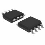 SH8M70TB1
The activity of extra discounts on wholesale prices is in full swing…
Please fill in your contact information and we will send you the latest wholesale price list.





