ChipApex | Global Electronic Components Supplier
SEARCH
Search Product
Search Post
— IC芯片 | 连接器 | 传感器 | 被动器件 —
Search productSearch post
— IC芯片 | 连接器 | 传感器 | 被动器件 —
Consult the customer manager about the wholesale price.
consultation hotline:86-132-6715-2157
email:[email protected]
Contact the product manager for consultation. One-stop consultation is available.
Do you want a lower wholesale price? Please send us your inquiry and we will reply immediately.
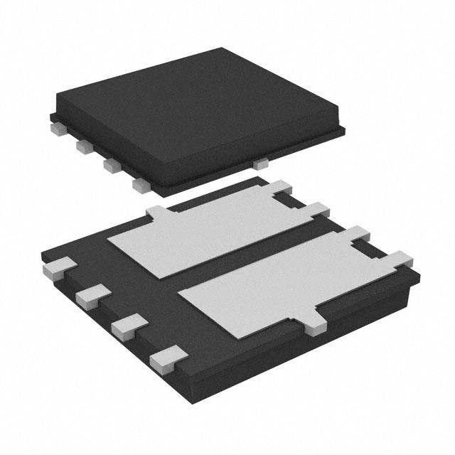
The Vishay Siliconix SI7214DN-T1-E3 is a dual N-Channel MOSFET utilizing TrenchFET technology, housed in a PowerPAK 1212-8 surface-mount package. It features a drain-source voltage (VDS) of 30 V and a gate-source voltage (VGS) of ±20 V. The device provides a maximum on-state resistance (RDS(on)) of 0.04 Ω at VGS = 10 V with a continuous drain current (ID) of 6.4 A, or 0.047 Ω at VGS = 4.5 V with an ID of 5.9 A. Key dynamic parameters include a total gate charge (Qg) of 4.2 nC, a turn-on delay time of 7.1 ns, and a fall time of 6 ns. Thermal ratings specify a maximum power dissipation of 2.6 W at 25 °C and a junction-to-case thermal resistance of 4.3 °C/W.
Verify the specific ordering suffix when sourcing components. The SI7214DN-T1-E3 designation indicates a lead-free product. Confirm whether halogen-free compliance is required for the project, as this corresponds to the GE3 suffix variant. Ensure that the procurement documentation matches the exact part number to avoid discrepancies in material specifications.
Select this component for space-constrained designs requiring dual N-channel switching capabilities. The low thermal impedance of the PowerPAK 1212-8 package supports efficient heat dissipation relative to its small footprint. Evaluate the 30 V rating against system voltage requirements and ensure the gate drive voltage aligns with the specified RDS(on) performance thresholds.
This component belongs to the Vishay Siliconix Si72 series of dual MOSFETs. It shares the PowerPAK 1212-8 package form factor with other devices in the lineup but is distinguished by its specific 30 V breakdown voltage and dual-channel architecture. The TrenchFET process technology differentiates it from standard planar MOSFETs.
Direct functional replacements must match the dual N-channel topology, 30 V rating, and PowerPAK 1212-8 pinout. Verify that any substitute maintains equivalent thermal resistance and gate charge characteristics to preserve circuit timing and efficiency.
The SI7214DN-T1-E3 is a lead-free version of the component. The SI7214DN-T1-GE3 variant includes both lead-free and halogen-free construction.
The on-state resistance increases as the gate-source voltage decreases. At VGS = 10 V, RDS(on) is typically 0.04 Ω, while at VGS = 4.5 V, it rises to 0.047 Ω.
 SI7214DN-T1-E3
The activity of extra discounts on wholesale prices is in full swing…
Please fill in your contact information and we will send you the latest wholesale price list.