ChipApex | Global Electronic Components Supplier
SEARCH
Search Product
Search Post
— IC芯片 | 连接器 | 传感器 | 被动器件 —
Search productSearch post
— IC芯片 | 连接器 | 传感器 | 被动器件 —
Consult the customer manager about the wholesale price.
consultation hotline:86-132-6715-2157
email:[email protected]
Contact the product manager for consultation. One-stop consultation is available.
Do you want a lower wholesale price? Please send us your inquiry and we will reply immediately.
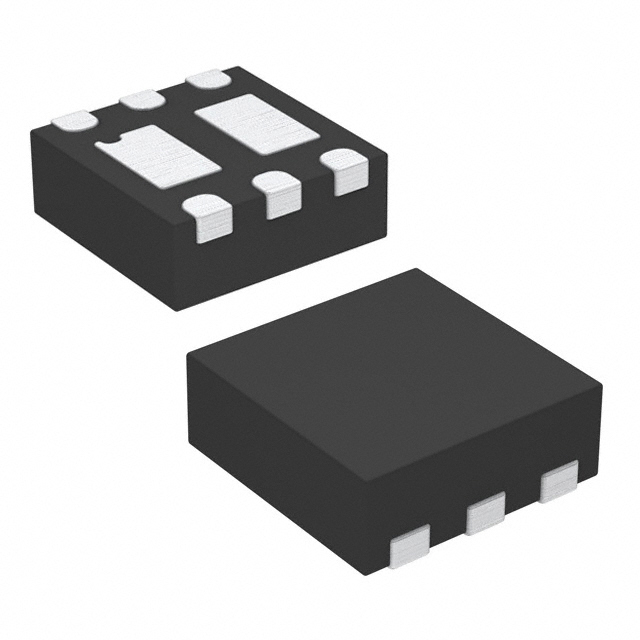
The Vishay Siliconix SiA517DJ-T1-GE3 is a dual N- and P-channel enhancement mode MOSFET utilizing TrenchFET technology. It features a thermally enhanced PowerPAK SC-70-6 package with dimensions of 2.05 mm by 2.05 mm. The device supports a drain-source voltage (VDS) of ±12 V and continuous drain current (ID) up to 4.5 A at TC = 25 °C. On-state resistance (RDS(on)) is specified at 0.029 Ω for the N-channel and 0.061 Ω for the P-channel at VGS = ±4.5 V. Maximum power dissipation reaches 6.5 W at TC = 25 °C, with an operating junction temperature range from -55 °C to +150 °C.
Verify component authenticity through authorized distributors or direct manufacturer channels. Confirm RoHS compliance and halogen-free status using official documentation. Validate lot traceability and date codes against current production records. Ensure storage conditions remain within specified limits to maintain solderability and electrical integrity prior to assembly.
Evaluate gate threshold voltage requirements against available drive voltages to ensure full enhancement. Consider thermal derating curves when designing for ambient temperatures exceeding 25 °C. Verify that peak pulsed currents remain within safe operating area limits defined in the datasheet characteristics.
This component belongs to the SiA series of TrenchFET MOSFETs manufactured by Vishay Siliconix. It utilizes the PowerPAK SC-70-6L dual pad package variant designed for surface mounting on FR4 substrates. The specific suffix -T1-GE3 indicates tape-and-reel packaging with lead-free and halogen-free compliant materials.
Direct functional substitutes within the same voltage and current ratings should be sourced from the Vishay SiA family. Verify pinout compatibility between the original PowerPAK SC-70-6 and potential replacement packages before integration into existing PCB layouts.
The absolute maximum rating for both N-channel and P-channel gate-source voltage (VGS) is ±8 V.
RDS(on) increases as gate voltage decreases. For the N-channel, it rises from 0.029 Ω at 4.5 V to 0.065 Ω at 1.5 V. For the P-channel, it increases from 0.061 Ω at -4.5 V to 0.170 Ω at -1.5 V.
Manual soldering with a soldering iron is not recommended for this leadless component due to the exposed copper tips resulting from singulation.
 SIA517DJ-T1-GE3
The activity of extra discounts on wholesale prices is in full swing…
Please fill in your contact information and we will send you the latest wholesale price list.