 ChipApex | Global Electronic Components Supplier
SEARCH
Search Product
Search Post
— IC芯片 | 连接器 | 传感器 | 被动器件 —
Search productSearch post
— IC芯片 | 连接器 | 传感器 | 被动器件 —
Consult the customer manager about the wholesale price.
consultation hotline:86-132-6715-2157
email:[email protected]
Contact the product manager for consultation. One-stop consultation is available.
Do you want a lower wholesale price? Please send us your inquiry and we will reply immediately.
The SMPJ109TR is a surface-mount N-channel JFET in an SOT-23 package, part of the InterFET J108/J109 series. It features a -25V Gate to Source Breakdown Voltage (BVGSS), a Drain to Source Saturation Current (IDSS) range of 40mA to 80mA, and a Gate to Source Cutoff Voltage (VGS(off)) between -2V and -6V. The device exhibits low noise with a typical value of 1 nV/√Hz and high gain at 100mS typical. Static characteristics include a maximum Gate to Source Reverse Current (IGSS) of -3nA and a Drain Cutoff Current (ID) of 3nA. Dynamic parameters specify Drain to Source ON Resistance (RDS(ON)) of 8Ω to 12Ω, input capacitance (Cgs) of 15pF, and drain-gate capacitance (Cgd) of 15pF at 1MHz. Maximum ratings allow for continuous power dissipation of 360mW and an operating junction temperature from -55°C to 125°C.
Verify the specific binning requirements for IDSS and VGS(off) against your circuit design needs, as these parameters vary within the specified ranges. Confirm that the tape and reel quantity aligns with production volume requirements. Ensure ESD handling procedures are followed during assembly, as bulk products are shipped in standard ESD material. Cross-reference the mechanical layout data with your PCB footprint design to ensure proper soldering and thermal management.
Select this component when low noise and high gain are critical for signal integrity in switching or commutator applications. Compare the IDSS and VGS(off) ranges against the J108 variant if higher saturation current is required. Consider the SOT-23 package constraints for thermal dissipation and board space. Verify compatibility with the intended supply voltage and signal levels to ensure operation within the specified breakdown and cutoff limits.
The SMPJ109TR belongs to the J108/J109 family of N-channel JFETs manufactured by InterFET. This series is engineered using proprietary N0450S geometry to deliver superior noise and gain characteristics compared to standard silicon JFETs. The product line offers multiple packaging options, including through-hole TO-92, surface mount SOT-23, and bare die configurations, catering to diverse manufacturing and application requirements.
The J108 is a direct pin-compatible alternative within the same series, offering different IDSS and VGS(off) characteristics. Verify electrical parameter alignment before substitution. No other cross-brand replacements are confirmed in the official documentation.
The typical noise figure is 1 nV/√Hz.
The maximum continuous power dissipation is 360 mW.
The operating junction temperature range is -55°C to 125°C.
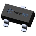 SMPJ109TR
The activity of extra discounts on wholesale prices is in full swing…
Please fill in your contact information and we will send you the latest wholesale price list.





