 ChipApex | Global Electronic Components Supplier

SEARCH
Search Product
Search Post
— IC芯片 | 连接器 | 传感器 | 被动器件 —
Search productSearch post
— IC芯片 | 连接器 | 传感器 | 被动器件 —
Consult the customer manager about the wholesale price.
consultation hotline:86-132-6715-2157
email:[email protected]
Contact the product manager for consultation. One-stop consultation is available.
Do you want a lower wholesale price? Please send us your inquiry and we will reply immediately.
SN74AVC4T245PWRG4 is listed in the Buffers, Drivers, Receivers, Transceivers range at ChipApex. The manufacturer field lists Texas Instruments. Its product description is IC TRANSLATION TXRX 3.6V 16TSSOP. Review the specifications below when checking this part for your BOM.
The SN74AVC4T245PWRG4 is a 4-bit dual-supply noninverting bus transceiver with configurable voltage translation and 3-state outputs. It operates within a supply voltage range of 1.2V to 3.6V on both VCCA and VCCB rails. The device supports asynchronous communication between two data buses, featuring maximum data rates up to 380Mbps for 1.8V to 3.3V translation. It includes Ioff circuitry for partial power-down mode and provides ESD protection exceeding JESD 22 standards.
Verify the package type matches the PW (TSSOP-16) designation in the ordering suffix. Confirm RoHS compliance and Green product status (no Sb/Br) as specified by the G4 suffix. Ensure the component meets the recommended operating conditions for VCCA and VCCB voltages before integration into the target system design.
Select this component when interfacing devices requiring bidirectional level translation between different low-voltage nodes such as 1.2V, 1.8V, 2.5V, and 3.3V. The device is suitable for applications needing push-pull drivers connected to data I/Os. Consider the TSSOP-16 package constraints and thermal characteristics if space or heat dissipation is a primary design factor.
This part belongs to the SN74AVC4T245 family of dual-bit bus transceivers. The PWRG4 suffix indicates a specific tape-and-reel packaging configuration in the PW (TSSOP-16) package. It shares functional specifications with other variants like SN74AVC4T245DT and SN74AVC4T245RGYR, differing primarily in physical package dimensions and manufacturing lot codes.
SN74AVC4T245DT
To ensure outputs remain in a high-impedance state during power-up or power-down, the OE input must be tied to VCCA through a pullup resistor. This prevents enabling the outputs until VCCA and VCCB are fully ramped and stable.
The Ioff feature supports partial-power-down mode operation. It disables the I/O output circuits to prevent backflow current through the device when it is powered down, protecting the system from damage.
Explore related parts through Logic, Integrated Circuits (ICs), all product categories, ChipApex homepage.
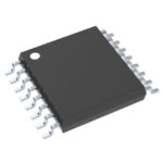 SN74AVC4T245PWRG4
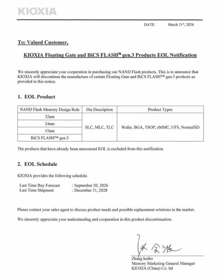
SN74AVC4T245PWRG4 is listed in the Buffers, Drivers, Receivers, Transceivers range at ChipApex. The manufacturer field lists Texas Instruments. Its product description is IC TRANSLATION…
Read More
SN74AVC4T245PWRG4 is listed in the Buffers, Drivers, Receivers, Transceivers range at ChipApex. The manufacturer field lists Texas Instruments. Its product description is IC TRANSLATION…
Read More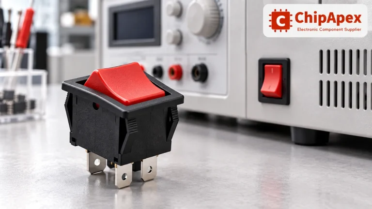
Choose a rocker switch by AC/DC ratings, contact arrangement, illumination, panel fit and sealing. Get practical checks for engineering and component sourcing.
Read More
SN74AVC4T245PWRG4 is listed in the Buffers, Drivers, Receivers, Transceivers range at ChipApex. The manufacturer field lists Texas Instruments. Its product description is IC TRANSLATION…
Read More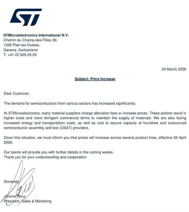
SN74AVC4T245PWRG4 is listed in the Buffers, Drivers, Receivers, Transceivers range at ChipApex. The manufacturer field lists Texas Instruments. Its product description is IC TRANSLATION…
Read More
SN74AVC4T245PWRG4 is listed in the Buffers, Drivers, Receivers, Transceivers range at ChipApex. The manufacturer field lists Texas Instruments. Its product description is IC TRANSLATION…
Read More
SN74AVC4T245PWRG4 is listed in the Buffers, Drivers, Receivers, Transceivers range at ChipApex. The manufacturer field lists Texas Instruments. Its product description is IC TRANSLATION…
Read More
SN74AVC4T245PWRG4 is listed in the Buffers, Drivers, Receivers, Transceivers range at ChipApex. The manufacturer field lists Texas Instruments. Its product description is IC TRANSLATION…
Read More
SN74AVC4T245PWRG4 is listed in the Buffers, Drivers, Receivers, Transceivers range at ChipApex. The manufacturer field lists Texas Instruments. Its product description is IC TRANSLATION…
Read More
SN74AVC4T245PWRG4 is listed in the Buffers, Drivers, Receivers, Transceivers range at ChipApex. The manufacturer field lists Texas Instruments. Its product description is IC TRANSLATION…
Read More
SN74AVC4T245PWRG4 is listed in the Buffers, Drivers, Receivers, Transceivers range at ChipApex. The manufacturer field lists Texas Instruments. Its product description is IC TRANSLATION…
Read More
SN74AVC4T245PWRG4 is listed in the Buffers, Drivers, Receivers, Transceivers range at ChipApex. The manufacturer field lists Texas Instruments. Its product description is IC TRANSLATION…
Read More
The activity of extra discounts on wholesale prices is in full swing…
Please fill in your contact information and we will send you the latest wholesale price list.





