 ChipApex | Global Electronic Components Supplier

SEARCH
Search Product
Search Post
— IC芯片 | 连接器 | 传感器 | 被动器件 —
Search productSearch post
— IC芯片 | 连接器 | 传感器 | 被动器件 —
Consult the customer manager about the wholesale price.
consultation hotline:86-132-6715-2157
email:[email protected]
Contact the product manager for consultation. One-stop consultation is available.
Do you want a lower wholesale price? Please send us your inquiry and we will reply immediately.
SN74HC126PW is listed in the Buffers, Drivers, Receivers, Transceivers range at ChipApex. The manufacturer field lists Texas Instruments. Its product description is IC BUFFER NON-INVERT 6V 14TSSOP. Review the specifications below when checking this part for your BOM.
The SN74HC126PW is a quadruple buffer with 3-state outputs manufactured by Texas Instruments. It operates within a supply voltage range of 2 V to 6 V and supports an operating temperature range from -40°C to +85°C. The device features buffered inputs, balanced CMOS outputs capable of sinking and sourcing similar currents, and standard high-impedance CMOS inputs. It provides fanout support for up to 10 LSTTL loads while offering significant power reduction compared to LSTTL logic ICs.
Verify the specific package type matches the design requirements, as the SN74HC126 family includes SOIC, SSOP, PDIP, SO, TSSOP, CDIP, and LCCC options. Confirm that the ordering suffix corresponds to the desired packaging format, such as tape and reel or tube, before finalizing procurement. Ensure compatibility with the intended operating temperature and voltage ranges specified in the datasheet.
Select this component when a non-inverting buffer with controllable output states is required. It is suitable for applications needing to drive multiple loads or manage bus lines where high-impedance isolation is necessary. Consider the thermal characteristics and load capacitance limits to ensure optimal performance and prevent damage due to over-current or excessive capacitive loading.
This device belongs to the SNx4HC126 series of quadruple buffers with 3-state outputs. It is part of the broader 74HC logic family, designed to provide low power consumption and high noise immunity. The PW designation specifically indicates the TSSOP (14-pin) package variant, which offers a compact form factor suitable for surface-mount applications.
SN74HC126D
Unused inputs must not be left floating; they should be terminated at either VCC or ground to prevent undefined operational states.
When disabled, the output enters a high-impedance state, neither sourcing nor sinking current, allowing the output voltage to be determined by the external circuit.
Explore related parts through Logic, Integrated Circuits (ICs), all product categories, ChipApex homepage.
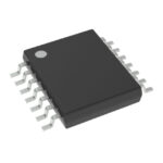 SN74HC126PW

SN74HC126PW is listed in the Buffers, Drivers, Receivers, Transceivers range at ChipApex. The manufacturer field lists Texas Instruments. Its product description is IC BUFFER…
Read More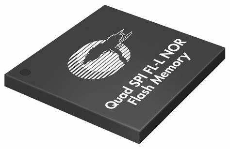
SN74HC126PW is listed in the Buffers, Drivers, Receivers, Transceivers range at ChipApex. The manufacturer field lists Texas Instruments. Its product description is IC BUFFER…
Read More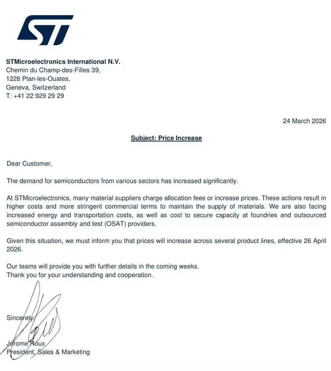
SN74HC126PW is listed in the Buffers, Drivers, Receivers, Transceivers range at ChipApex. The manufacturer field lists Texas Instruments. Its product description is IC BUFFER…
Read More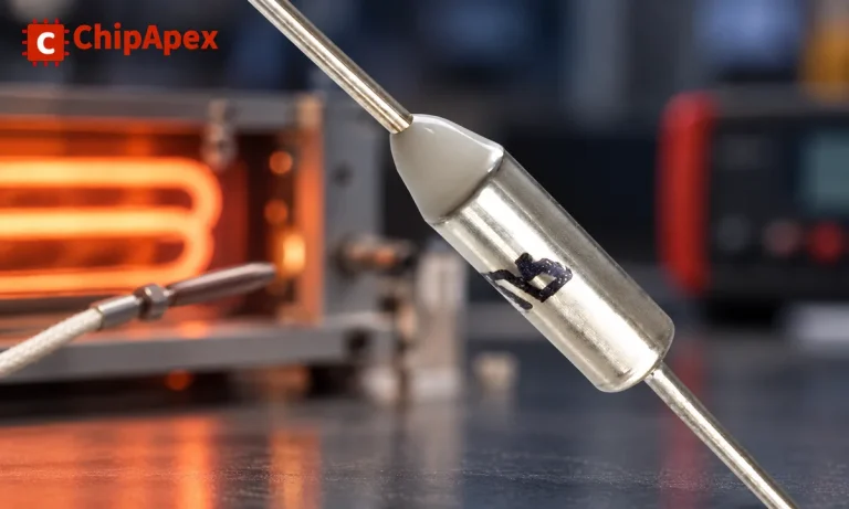
Understand thermal fuse operation, Tf, Th and Tm, electrical ratings and mounting. Check temperature limits and replacement requirements for your design.
Read More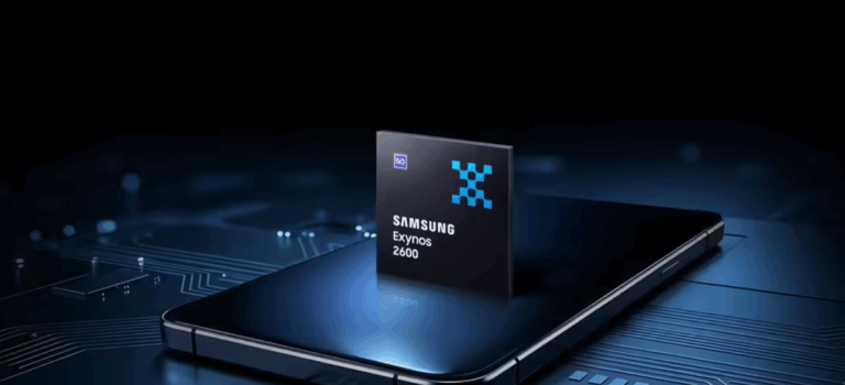
SN74HC126PW is listed in the Buffers, Drivers, Receivers, Transceivers range at ChipApex. The manufacturer field lists Texas Instruments. Its product description is IC BUFFER…
Read More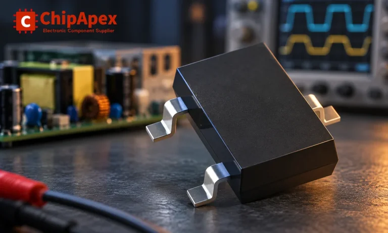
Learn how rectifiers convert AC to DC, compare half-wave and bridge circuits, and select voltage, current, recovery and thermal ratings for your design.
Read More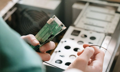
SN74HC126PW is listed in the Buffers, Drivers, Receivers, Transceivers range at ChipApex. The manufacturer field lists Texas Instruments. Its product description is IC BUFFER…
Read More
SN74HC126PW is listed in the Buffers, Drivers, Receivers, Transceivers range at ChipApex. The manufacturer field lists Texas Instruments. Its product description is IC BUFFER…
Read More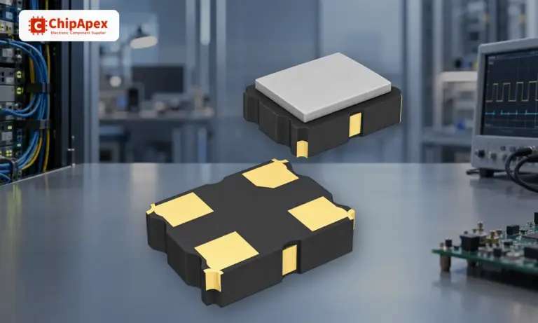
Understand how oscillators generate timing signals, how they differ from crystals, and which frequency, output and stability specs matter when choosing one.
Read More
SN74HC126PW is listed in the Buffers, Drivers, Receivers, Transceivers range at ChipApex. The manufacturer field lists Texas Instruments. Its product description is IC BUFFER…
Read More
SN74HC126PW is listed in the Buffers, Drivers, Receivers, Transceivers range at ChipApex. The manufacturer field lists Texas Instruments. Its product description is IC BUFFER…
Read More
SN74HC126PW is listed in the Buffers, Drivers, Receivers, Transceivers range at ChipApex. The manufacturer field lists Texas Instruments. Its product description is IC BUFFER…
Read More
The activity of extra discounts on wholesale prices is in full swing…
Please fill in your contact information and we will send you the latest wholesale price list.





