ChipApex | Global Electronic Components Supplier

SEARCH
Search Product
Search Post
— IC芯片 | 连接器 | 传感器 | 被动器件 —
Search productSearch post
— IC芯片 | 连接器 | 传感器 | 被动器件 —
Consult the customer manager about the wholesale price.
consultation hotline:86-132-6715-2157
email:[email protected]
Contact the product manager for consultation. One-stop consultation is available.
Do you want a lower wholesale price? Please send us your inquiry and we will reply immediately.
SN74SSTVF16857GR is listed in the Specialty Logic range at ChipApex. The manufacturer field lists Texas Instruments. Its product description is IC REG BUFF 14BIT SSTL 48-TSSOP. Review the specifications below when checking this part for your BOM.
The SN74SSTVF16857GR is a 14-bit registered buffer designed for 2.3-V to 2.7-V VCC operation, belonging to the Widebus family. It features SSTL_2 data inputs and outputs meeting SSTL_2 Class I specifications. The device operates from differential clock inputs (CLK and CLK), registering data at the crossing of CLK going high and CLK going low. It supports LVCMOS switching levels on the RESET input, which disables differential receivers and forces all outputs low when active. The flow-through architecture optimizes PCB layout.
Verify the specific ordering suffix 'GR' corresponds to the TSSOP-48 package in tape and reel format with 2000 units per reel. Confirm that the component status is listed as Active Production. Ensure the operating temperature range matches the required application environment of 0°C to 70°C. Check for RoHS compliance and lead finish details such as NIPDAU.
Select this component for designs requiring 14-bit registered buffering with SSTL_2 compatibility. It is suitable for systems operating between 2.3 V and 2.7 V. Consider its flow-through architecture for simplified PCB layout. Verify that the differential clock requirements align with the system's timing constraints. Ensure the RESET input logic levels match the LVCMOS standard used in the design.
This part is part of Texas Instruments' Widebus family, specifically the SN74SSTVF16857 series. It is pinout and functionality compatible with the JEDEC standard SSTV16857. The device is manufactured by Texas Instruments and falls under the category of buffers and line drivers within their logic IC portfolio.
The SN74SSTVF16857GR is functionally compatible with the JEDEC standard SSTV16857. Designers should verify pinout compatibility before substitution. No other specific replacement part numbers are documented in the provided source material.
When the RESET input is low, it disables the differential input receivers, resets all registers, and forces all outputs low. Undriven (floating) data, clock, and reference voltage inputs are allowed during this state.
For PC1600, PC2100, and PC2700 applications, the VDDQ range is 2.3 V to 2.7 V. For PC3200 applications, the VDDQ range is 2.5 V to 2.7 V.
Yes, the output edge-control circuitry minimizes switching noise in unterminated DIMM loads. It operates up to 600 ps faster than the JEDEC standard SSTV16857 in PC2700 DIMM applications regarding simultaneous switching.
Explore related parts through Logic, Integrated Circuits (ICs), all product categories, ChipApex homepage.
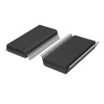 SN74SSTVF16857GR
SN74SSTVF16857GR is listed in the Specialty Logic range at ChipApex. The manufacturer field lists Texas Instruments. Its product description is IC REG BUFF 14BIT…
Read More
SN74SSTVF16857GR is listed in the Specialty Logic range at ChipApex. The manufacturer field lists Texas Instruments. Its product description is IC REG BUFF 14BIT…
Read More
SN74SSTVF16857GR is listed in the Specialty Logic range at ChipApex. The manufacturer field lists Texas Instruments. Its product description is IC REG BUFF 14BIT…
Read More
Explore electronic component types, functions, packages and datasheets. Learn selection, replacement and BOM checks before ordering parts for your PCB.
Read More
SN74SSTVF16857GR is listed in the Specialty Logic range at ChipApex. The manufacturer field lists Texas Instruments. Its product description is IC REG BUFF 14BIT…
Read More
SN74SSTVF16857GR is listed in the Specialty Logic range at ChipApex. The manufacturer field lists Texas Instruments. Its product description is IC REG BUFF 14BIT…
Read More
Choose LED drivers by current, string voltage, dimming and thermal limits. Understand constant-current operation and the checks needed for your load.
Read More
SN74SSTVF16857GR is listed in the Specialty Logic range at ChipApex. The manufacturer field lists Texas Instruments. Its product description is IC REG BUFF 14BIT…
Read More
SN74SSTVF16857GR is listed in the Specialty Logic range at ChipApex. The manufacturer field lists Texas Instruments. Its product description is IC REG BUFF 14BIT…
Read More
Learn what data acquisition means, from sensors and conditioning to sampling and storage. Review channel timing, wiring, calibration and data quality.
Read More
SN74SSTVF16857GR is listed in the Specialty Logic range at ChipApex. The manufacturer field lists Texas Instruments. Its product description is IC REG BUFF 14BIT…
Read More
SN74SSTVF16857GR is listed in the Specialty Logic range at ChipApex. The manufacturer field lists Texas Instruments. Its product description is IC REG BUFF 14BIT…
Read More
The activity of extra discounts on wholesale prices is in full swing…
Please fill in your contact information and we will send you the latest wholesale price list.