 ChipApex | Global Electronic Components Supplier
SEARCH
Search Product
Search Post
— IC芯片 | 连接器 | 传感器 | 被动器件 —
Search productSearch post
— IC芯片 | 连接器 | 传感器 | 被动器件 —
Consult the customer manager about the wholesale price.
consultation hotline:86-132-6715-2157
email:[email protected]
Contact the product manager for consultation. One-stop consultation is available.
Do you want a lower wholesale price? Please send us your inquiry and we will reply immediately.
The SP8K31TB1 is a dual N-channel silicon MOSFET in an SOP8 surface-mount package. It features a drain-source voltage of 60V and a continuous drain current of ±3.5A. The device includes built-in gate-source protection diodes and body diodes. Electrical characteristics include a typical RDS(on) of 85mΩ at VGS=10V, 105mΩ at VGS=4.5V, and 120mΩ at VGS=4.0V, all measured at ID=3.5A. Total gate charge (Qg) is typically 3.7nC. Power dissipation is rated at 2.0W, with a channel temperature limit of 150°C and a storage temperature range of -55°C to +150°C.
Verify the specific ordering suffix TB against official documentation to confirm taping packaging details. Confirm availability status as the base model may have lifecycle restrictions. Ensure design compliance with absolute maximum ratings during procurement planning.
Select this component for low-voltage switching circuits requiring dual N-channel isolation in a small footprint. Evaluate RDS(on) performance at the specific drive voltage intended for the application. Consider thermal derating for power dissipation limits above ambient temperatures.
The SP8K31TB1 belongs to ROHM's 4V drive N-channel MOSFET series. It utilizes silicon N-channel structure technology designed for efficient switching operations. The SOP8 package provides a standardized form factor for automated surface-mount assembly processes.
SP8K31HZG is documented as a replacement with the same pinout and package.
It protects the gate-source terminals against static electricity damage when the product is in use.
The Drain-Source Voltage (VDS) is 60V, and the Gate-Source Voltage (VGS) is ±20V.
RDS(on) is typically 85mΩ at VGS=10V, 105mΩ at VGS=4.5V, and 120mΩ at VGS=4.0V, measured at ID=3.5A.
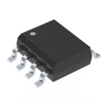 SP8K31TB1
The activity of extra discounts on wholesale prices is in full swing…
Please fill in your contact information and we will send you the latest wholesale price list.





