ChipApex | Global Electronic Components Supplier
SEARCH
Search Product
Search Post
— IC芯片 | 连接器 | 传感器 | 被动器件 —
Search productSearch post
— IC芯片 | 连接器 | 传感器 | 被动器件 —
Consult the customer manager about the wholesale price.
consultation hotline:86-132-6715-2157
email:[email protected]
Contact the product manager for consultation. One-stop consultation is available.
Do you want a lower wholesale price? Please send us your inquiry and we will reply immediately.
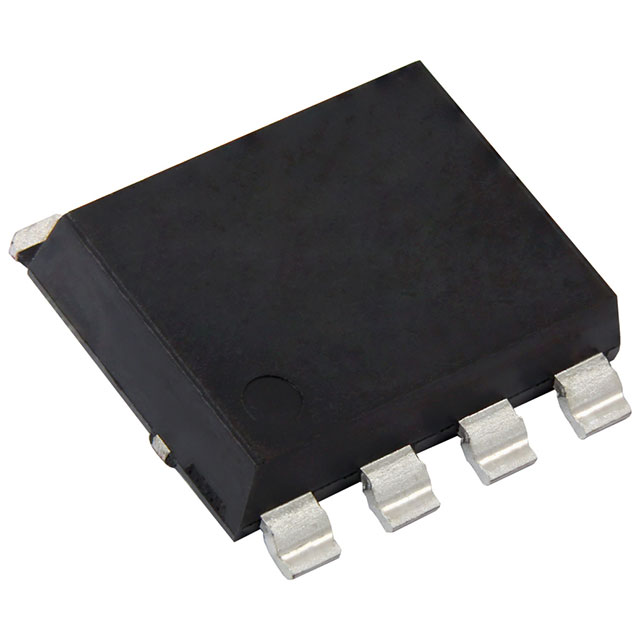
The Vishay Siliconix SQJ740EP-T1_GE3 is an automotive-grade dual N-channel enhancement mode MOSFET utilizing TrenchFET Gen IV technology. It features a 40 V drain-source voltage rating and operates within a junction temperature range of -55 °C to +175 °C. The device provides a maximum on-state resistance (RDS(on)) of 3.4 mΩ at VGS = 10 V, with a typical value of 2.8 mΩ. Each channel supports a continuous drain current of 123 A at TC = 25 °C and a pulsed drain current of 399 A. Packaged in a PowerPAK SO-8L Dual BWL surface-mount footprint, it includes an integrated body diode with a forward voltage of 1.2 V max at IF = 7 A.
Verify the specific ordering suffix against official documentation to confirm package type and lead-free status. Ensure compliance with RoHS directives by checking material categorization reports. Confirm that the component meets AEC-Q101 requirements for your specific automotive application environment before finalizing procurement.
Select this component when a compact dual N-channel solution is required for 40 V automotive circuits. Evaluate thermal performance based on the specified RthJC of 1.6 °C/W and ensure PCB layout supports the PowerPAK SO-8L footprint. Consider the total gate charge of 56 nTyp for driver compatibility in high-frequency switching applications.
This part belongs to the SQJ series of Vishay Siliconix TrenchFET MOSFETs designed for automotive environments. It shares the PowerPAK SO-8L Dual BWL package form factor with other dual-channel variants in the lineup, offering a space-efficient alternative to discrete single-channel packages for balanced load applications.
Direct replacements must match the 40 V rating, dual N-channel configuration, and PowerPAK SO-8L Dual BWL package. Verify that any substitute maintains equivalent RDS(on) limits and AEC-Q101 qualification if automotive reliability is required.
The maximum pulsed drain current (IDM) is 399 A, measured under pulse test conditions with a width of ≤ 300 μs and duty cycle ≤ 2%.
Yes, the device is AEC-Q101 qualified and rated for an operating junction temperature range from -55 °C to +175 °C.
The body diode reverse recovery time (trr) is typically 346 ns when tested at IF = 7 A and di/dt = 100 A/μs.
 SQJ740EP-T1_GE3
The activity of extra discounts on wholesale prices is in full swing…
Please fill in your contact information and we will send you the latest wholesale price list.