ChipApex | Global Electronic Components Supplier
SEARCH
Search Product
Search Post
— IC芯片 | 连接器 | 传感器 | 被动器件 —
Search productSearch post
— IC芯片 | 连接器 | 传感器 | 被动器件 —
Consult the customer manager about the wholesale price.
consultation hotline:86-132-6715-2157
email:[email protected]
Contact the product manager for consultation. One-stop consultation is available.
Do you want a lower wholesale price? Please send us your inquiry and we will reply immediately.
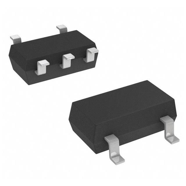
The SSM5N16FU is a dual N-channel silicon MOSFET in a compact SOT-353-5 package. It features a drain-source breakdown voltage of 20 V and a continuous drain current of 100 mA. The device offers low on-resistance, specified as 3.0 Ω max at VGS = 4 V, 4.0 Ω max at VGS = 2.5 V, and 15 Ω max at VGS = 1.5 V. Gate threshold voltage ranges from 0.6 V to 1.1 V. Total power dissipation is rated at 200 mW at 25°C ambient temperature, with a maximum channel temperature of 150°C.
Verify the specific ordering suffix against official Toshiba Semiconductor and Storage documentation to ensure correct packaging and compliance status. Confirm that the component meets all environmental regulations required for the target market. Review the manufacturer's reliability handbook for derating guidelines before finalizing procurement specifications.
Select this component for circuits requiring dual N-channel MOSFETs in small form factors. Ensure the gate drive voltage aligns with the desired on-resistance performance, as RDS(on) varies significantly between 1.5 V and 4 V thresholds. Verify that the 20 V breakdown voltage and 100 mA current limits accommodate the peak operational demands of the application.
This device belongs to Toshiba's line of silicon N-channel field effect transistors designed for general-purpose switching. The SSM5N16FU integrates two independent channels in a single surface-mount package, reducing board space compared to discrete solutions. It serves as a compact alternative for low-voltage signal routing and logic level switching tasks.
Consult official Toshiba substitution guides for verified equivalents. Do not assume pin-compatible alternatives without verifying electrical parameters such as RDS(on) and V(BR)DSS against the original datasheet requirements.
 SSM5N16FU,LF
The activity of extra discounts on wholesale prices is in full swing…
Please fill in your contact information and we will send you the latest wholesale price list.