ChipApex | Global Electronic Components Supplier
SEARCH
Search Product
Search Post
— IC芯片 | 连接器 | 传感器 | 被动器件 —
Search productSearch post
— IC芯片 | 连接器 | 传感器 | 被动器件 —
Consult the customer manager about the wholesale price.
consultation hotline:86-132-6715-2157
email:[email protected]
Contact the product manager for consultation. One-stop consultation is available.
Do you want a lower wholesale price? Please send us your inquiry and we will reply immediately.
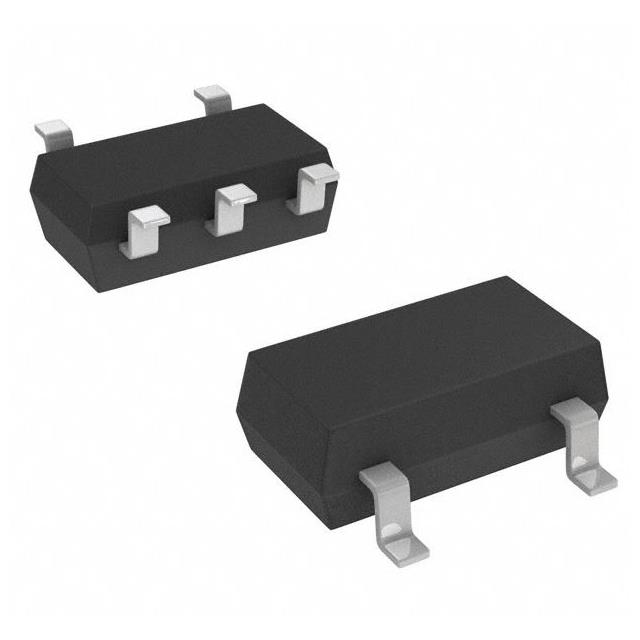
The SSM5P15FU,LF is a dual P-channel MOSFET manufactured by Toshiba Semiconductor and Storage. It features a compact UFV package with five terminals. The device supports a drain-source voltage of -30 V and a continuous drain current of -100 mA. At VGS = -4 V, the maximum on-resistance is 12 Ω, while at VGS = -2.5 V, it reaches 32 Ω. The gate threshold voltage ranges from -1.1 V to -1.7 V. Power dissipation is rated at 200 mW at 25°C. Switching times include a turn-on time of 65 ns and a turn-off time of 175 ns under standard test conditions.
Verify the specific ordering suffix against official Toshiba documentation to confirm packaging type and environmental compliance status. Confirm that the component meets RoHS directives if required by your manufacturing standards. Ensure electrostatic discharge precautions are observed during handling, as specified in the manufacturer's handling guidelines.
Select this component when a dual P-channel MOSFET solution is required in a minimal footprint. Evaluate the on-resistance requirements at your specific gate drive voltage, as performance varies significantly between -2.5 V and -4 V logic levels. Consider the thermal derating curves provided in the datasheet to ensure power dissipation limits are not exceeded in your target operating environment.
This part belongs to Toshiba's silicon P-channel MOSFET series designed for general-purpose switching. It utilizes the UFV surface-mount package, which provides a compact form factor suitable for portable electronics and dense PCB layouts. The dual structure allows for independent control of two channels within a single physical housing.
Direct replacements must match the dual P-channel topology, -30 V rating, and UFV-5 pinout. Verify that alternative components offer comparable on-resistance at your intended gate drive voltage and similar switching speeds to maintain circuit timing integrity.
The on-resistance is 12 Ω maximum at VGS = -4 V, but increases to 32 Ω maximum at VGS = -2.5 V.
The gate threshold voltage (Vth) is measured at a drain current (ID) of -0.1 mA with a drain-source voltage (VDS) of -3 V, ranging from -1.1 V to -1.7 V.
Under test conditions of VDD = -5 V and ID = -10 mA, the typical turn-on time is 65 ns and the typical turn-off time is 175 ns.
 SSM5P15FU,LF
The activity of extra discounts on wholesale prices is in full swing…
Please fill in your contact information and we will send you the latest wholesale price list.