 ChipApex | Global Electronic Components Supplier
SEARCH
Search Product
Search Post
— IC芯片 | 连接器 | 传感器 | 被动器件 —
Search productSearch post
— IC芯片 | 连接器 | 传感器 | 被动器件 —
Consult the customer manager about the wholesale price.
consultation hotline:86-132-6715-2157
email:[email protected]
Contact the product manager for consultation. One-stop consultation is available.
Do you want a lower wholesale price? Please send us your inquiry and we will reply immediately.
The SSM6L40TU,LF is a dual MOSFET from Toshiba featuring one N-channel and one P-channel enhancement-mode transistor in a UF-6 surface-mount package. It utilizes U-MOSIII technology for low on-resistance. Key electrical parameters include a drain-source breakdown voltage (Vds) of 30 V, continuous drain current (Id) ranging from 1.4 A to 1.6 A, and gate-source voltage (Vgs) limits of ±20 V. The device exhibits on-resistances (Rds(on)) of 122 mΩ and 226 mΩ, with gate charges (Qg) of 5.1 nC and 2.9 nC respectively. Threshold voltages (Vgs(th)) are specified between 1 V and 2 V. Power dissipation is rated at 500 mW, with an operating temperature range of -55°C to +150°C.
Verify the specific ordering suffix when sourcing. The base model SSM6L40TU,LF differs from variants such as SSM6L40TU(TE85L,F), which indicates a specific tape-and-reel packaging format. Confirm that the required package style matches the project specifications before procurement to ensure compatibility with assembly processes.
Select this component for designs requiring a matched N/P pair in a minimal footprint. The 30 V rating supports 12 V nominal systems. Ensure thermal management accommodates the 500 mW power dissipation limit. Verify that the gate charge values align with the driving circuit's speed requirements for efficient switching performance.
This part belongs to the SSM6L40TU series of dual MOSFETs manufactured by Toshiba Semiconductor and Storage. It is distinct from other series like SSM6J424TU or SSM6P36TU, which feature different voltage ratings, current capacities, or channel configurations. The UF-6 package provides a compact solution compared to larger discrete packages.
Direct substitutes must match the UF-6 package, 30 V rating, and dual N/P configuration. Verify pinout compatibility and electrical parameters against alternative dual MOSFETs from other manufacturers before implementation.
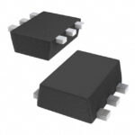 SSM6L40TU,LF
The activity of extra discounts on wholesale prices is in full swing…
Please fill in your contact information and we will send you the latest wholesale price list.





