ChipApex | Global Electronic Components Supplier
SEARCH
Search Product
Search Post
— IC芯片 | 连接器 | 传感器 | 被动器件 —
Search productSearch post
— IC芯片 | 连接器 | 传感器 | 被动器件 —
Consult the customer manager about the wholesale price.
consultation hotline:86-132-6715-2157
email:[email protected]
Contact the product manager for consultation. One-stop consultation is available.
Do you want a lower wholesale price? Please send us your inquiry and we will reply immediately.
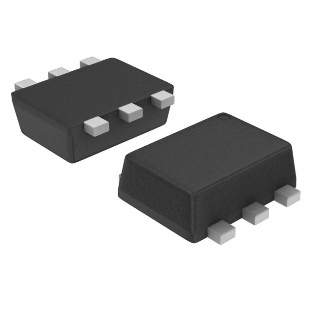
The SSM6N16FE,L3F is a dual N-channel silicon MOSFET from Toshiba, packaged in the compact ES-6 (SOT-563) form factor. It features a drain-source voltage rating of 20 V and a continuous drain current of 100 mA. The device exhibits low on-resistance values of 3.0 Ω max at VGS = 4 V, 4.0 Ω max at VGS = 2.5 V, and 15 Ω max at VGS = 1.5 V. Key electrical parameters include a gate threshold voltage range of 0.6 V to 1.1 V, forward transfer admittance of 40 mS, and input capacitance of 9.3 pF. Switching performance includes turn-on and turn-off times of 70 ns and 125 ns respectively. Total power dissipation is rated at 150 mW with a maximum channel temperature of 150 °C.
Verify the specific ordering suffix L3F against official Toshiba documentation to confirm tape-and-reel packaging specifications. Ensure compatibility with RoHS directives and confirm the manufacturer source directly from Toshiba Electronic Devices & Storage Corporation or authorized distributors. Validate that the ES-6 package dimensions match your PCB layout requirements before finalizing procurement orders.
Select this component when space constraints necessitate a dual N-channel MOSFET in an SMD package. Consider the 20 V breakdown voltage and 100 mA current limits for appropriate load matching. Evaluate the gate drive voltage levels required to achieve the desired on-resistance, as Ron varies significantly between 1.5 V and 4 V gate thresholds. Ensure thermal management supports the 150 mW dissipation rating under operating conditions.
This part belongs to Toshiba's small-signal MOSFET portfolio designed for portable electronics. The SSM6N16FE utilizes the ES-6 package to provide two independent N-channel transistors in a minimal footprint. It serves as a discrete solution for signal routing and switching tasks where board area is limited but dual-channel functionality is required.
Direct pin-compatible replacements within the same ES-6 package should be evaluated based on matching VDS, ID, and Ron specifications. Verify that any substitute maintains similar switching times and capacitance values to ensure circuit timing integrity without redesign.
 SSM6N16FE,L3F
The activity of extra discounts on wholesale prices is in full swing…
Please fill in your contact information and we will send you the latest wholesale price list.