ChipApex | Global Electronic Components Supplier
SEARCH
Search Product
Search Post
— IC芯片 | 连接器 | 传感器 | 被动器件 —
Search productSearch post
— IC芯片 | 连接器 | 传感器 | 被动器件 —
Consult the customer manager about the wholesale price.
consultation hotline:86-132-6715-2157
email:[email protected]
Contact the product manager for consultation. One-stop consultation is available.
Do you want a lower wholesale price? Please send us your inquiry and we will reply immediately.
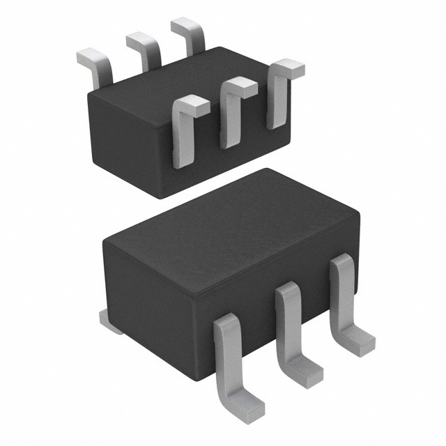
The SSM6N7002BFU is a dual N-channel silicon MOSFET utilizing Toshiba U-MOS IV technology, housed in a compact US6 surface-mount package. It features a drain-source voltage rating of 60 V and a continuous drain current of 200 mA. The device offers low on-resistance values of 3.3 Ω (max) at VGS = 4.5 V, 2.6 Ω (max) at VGS = 5 V, and 2.1 Ω (max) at VGS = 10 V. Electrical characteristics include a gate threshold voltage range of 1.5 V to 3.1 V, a maximum gate leakage current of ±10 μA, and a total power dissipation of 300 mW at 25°C ambient temperature.
Verify the specific ordering suffix against the manufacturer's official documentation to confirm packaging format and tape-and-reel specifications. Confirm RoHS compliance status and environmental declarations directly with the supplier or distributor prior to procurement. Ensure that the component version matches the required reliability standards for the intended application environment.
Select this component when a dual N-channel configuration is required in a minimal space-constrained layout. Evaluate the 60V breakdown voltage and 200mA current limits against circuit requirements. Consider the RDS(ON) variations across different gate drive voltages (4.5V, 5V, 10V) to ensure adequate drive levels are available for optimal conduction performance.
This part belongs to Toshiba's small-signal MOSFET portfolio designed for general-purpose switching. It utilizes the US6 (SC-88) package, which is standard for low-power surface-mount applications. The device represents an evolution in small-package FETs, balancing electrical performance with physical size constraints typical in modern consumer electronics.
Check for direct pin-compatible alternatives within the same series or similar packages. Verify that any substitute maintains the 60V VDS rating and comparable RDS(ON) characteristics. Ensure the replacement supports the required switching speeds and thermal dissipation capabilities for the specific board layout.
 SSM6N7002BFU(T5L,F
The activity of extra discounts on wholesale prices is in full swing…
Please fill in your contact information and we will send you the latest wholesale price list.