 ChipApex | Global Electronic Components Supplier
SEARCH
Search Product
Search Post
— IC芯片 | 连接器 | 传感器 | 被动器件 —
Search productSearch post
— IC芯片 | 连接器 | 传感器 | 被动器件 —
Consult the customer manager about the wholesale price.
consultation hotline:86-132-6715-2157
email:[email protected]
Contact the product manager for consultation. One-stop consultation is available.
Do you want a lower wholesale price? Please send us your inquiry and we will reply immediately.
The TPS2013APWR is a high-side power distribution switch from the TPS201xA family, designed for applications involving heavy capacitive loads and short circuits. It features an N-channel MOSFET with a typical on-resistance of 33 mΩ at 5 V input. The device operates within an input voltage range of 2.7 V to 5.5 V and provides a continuous output current capability up to 1.5 A. It incorporates an internal charge pump for gate drive control, enabling operation without external components. Key protection mechanisms include fixed current limiting, thermal shutdown with automatic recovery, and undervoltage lockout. The component is housed in a 14-pin TSSOP package and supports an ambient temperature range of -40°C to 85°C.
Verify the specific ordering suffix against the manufacturer's Package Option Addendum to confirm the tape and reel quantity and moisture sensitivity level. Ensure the selected variant matches the required operating temperature range and package dimensions for the target PCB layout. Cross-reference the active status and lead finish specifications with current production data sheets before finalizing procurement orders.
Select the TPS2013APWR when a higher short-circuit current threshold is required compared to lower-rated variants in the TPS201xA family. Evaluate the thermal resistance of the TSSOP-14 package against expected power dissipation levels under continuous load conditions. Confirm that the logic-level enable input compatibility aligns with the system's control voltage standards for reliable switching operation.
The TPS2013APWR belongs to the TPS201xA series of power distribution switches manufactured by Texas Instruments. This family differentiates devices primarily by their short-circuit current limit thresholds, ranging from 0.2 A to 2.2 A. The TPS2013A variant specifically targets applications requiring a 2.2 A typical current limit, distinguishing it from the TPS2010A, TPS2011A, and TPS2012A models within the same functional architecture.
Direct substitutes within the TPS201xA family include TPS2010AD, TPS2011AD, and TPS2012AD, which share identical pinouts and protection features but differ in current limit ratings. Verify that the alternative part number meets the specific load current requirements of the design.
When a short circuit is detected, the device limits the output current to a safe level by entering a constant-current mode. If the overload persists and causes the junction temperature to rise significantly, the thermal protection circuit will shut off the switch to prevent damage.
The internal charge pump supplies the necessary voltage to drive the gate of the N-channel MOSFET above the source voltage. It also controls the rise and fall times of the output voltage to minimize current surges and reduce electromagnetic interference during switching events.
No, the device is designed without a drain-source back-gate diode, which prevents reverse current flow from the output to the input when the switch is disabled.
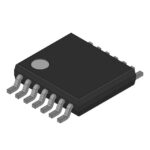 TPS2013APWR
The activity of extra discounts on wholesale prices is in full swing…
Please fill in your contact information and we will send you the latest wholesale price list.





