 ChipApex | Global Electronic Components Supplier

SEARCH
Search Product
Search Post
— IC芯片 | 连接器 | 传感器 | 被动器件 —
Search productSearch post
— IC芯片 | 连接器 | 传感器 | 被动器件 —
Consult the customer manager about the wholesale price.
consultation hotline:86-132-6715-2157
email:[email protected]
Contact the product manager for consultation. One-stop consultation is available.
Do you want a lower wholesale price? Please send us your inquiry and we will reply immediately.
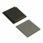
XCV400E-6FG676C is listed in the Field Programmable Gate Array range at ChipApex. The manufacturer field lists AMD. Its product description is IC FPGA 404 I/O 676FCBGA. Review the specifications below when checking this part for your BOM.
The XCV400E-6FG676C is a Virtex-E Field Programmable Gate Array manufactured by AMD (Xilinx). It features 129,600 logic gates and 10,800 configurable logic blocks (CLBs) within a 40x60 array. The device includes 163,840 bits of Block SelectRAM and 153,600 bits of distributed RAM. It operates at a maximum internal frequency of 130 MHz with four LUT levels and supports up to 404 user I/Os in the FG676 package. The core voltage is 1.8 V, while I/O banks support 3.3 V standards.
Verify the specific speed grade suffix (-6) against the design timing requirements, as other grades exist for this device family. Confirm that the FG676 Fine Pitch Ball Grid Array package dimensions match the PCB footprint constraints. Ensure the development environment supports the Virtex-E architecture, as bitstreams are not compatible with standard Virtex devices.
Select this component when designs require high-density logic combined with substantial block memory resources. The Virtex-E family offers improved performance over previous generations, specifically regarding I/O speeds and internal clocking capabilities. Consider the 1.8 V core voltage requirements for power budgeting and the availability of 3.3 V tolerant I/Os for system interfacing.
This part belongs to the Virtex-E 1.8 V FPGA family, which utilizes an advanced 0.18 μm six-layer metal CMOS process. This manufacturing technology enables smaller die sizes, faster switching speeds, and lower power consumption compared to earlier 2.5 V Virtex devices. The family ranges from 58 k to 4 M system gates.
The XCV400E-6FG676C is not bitstream-compatible with the original Virtex family. While pin-compatible with some exceptions, designs must be recompiled for Virtex-E. No direct functional substitutes are listed in the provided documentation; migration to larger devices like the XCV600E requires checking VREF and VCCO pin mappings.
Explore related parts through Embedded, Integrated Circuits (ICs), all product categories, ChipApex homepage.


 XCV400E-6FG676C

XCV400E-6FG676C is listed in the Field Programmable Gate Array range at ChipApex. The manufacturer field lists AMD. Its product description is IC FPGA 404…
Read More
XCV400E-6FG676C is listed in the Field Programmable Gate Array range at ChipApex. The manufacturer field lists AMD. Its product description is IC FPGA 404…
Read More
XCV400E-6FG676C is listed in the Field Programmable Gate Array range at ChipApex. The manufacturer field lists AMD. Its product description is IC FPGA 404…
Read More
See how a MEMS gyroscope measures angular rate, why its angle estimate drifts, and which range, noise, interface and temperature specs to compare.
Read More
XCV400E-6FG676C is listed in the Field Programmable Gate Array range at ChipApex. The manufacturer field lists AMD. Its product description is IC FPGA 404…
Read More
XCV400E-6FG676C is listed in the Field Programmable Gate Array range at ChipApex. The manufacturer field lists AMD. Its product description is IC FPGA 404…
Read More
XCV400E-6FG676C is listed in the Field Programmable Gate Array range at ChipApex. The manufacturer field lists AMD. Its product description is IC FPGA 404…
Read More
XCV400E-6FG676C is listed in the Field Programmable Gate Array range at ChipApex. The manufacturer field lists AMD. Its product description is IC FPGA 404…
Read More
XCV400E-6FG676C is listed in the Field Programmable Gate Array range at ChipApex. The manufacturer field lists AMD. Its product description is IC FPGA 404…
Read More
XCV400E-6FG676C is listed in the Field Programmable Gate Array range at ChipApex. The manufacturer field lists AMD. Its product description is IC FPGA 404…
Read More
XCV400E-6FG676C is listed in the Field Programmable Gate Array range at ChipApex. The manufacturer field lists AMD. Its product description is IC FPGA 404…
Read More
XCV400E-6FG676C is listed in the Field Programmable Gate Array range at ChipApex. The manufacturer field lists AMD. Its product description is IC FPGA 404…
Read More
The activity of extra discounts on wholesale prices is in full swing…
Please fill in your contact information and we will send you the latest wholesale price list.



