 ChipApex | Global Electronic Components Supplier

SEARCH
Search Product
Search Post
— IC芯片 | 连接器 | 传感器 | 被动器件 —
Search productSearch post
— IC芯片 | 连接器 | 传感器 | 被动器件 —
Consult the customer manager about the wholesale price.
consultation hotline:86-132-6715-2157
email:[email protected]
Contact the product manager for consultation. One-stop consultation is available.
Do you want a lower wholesale price? Please send us your inquiry and we will reply immediately.
XCVU9P-2FLGC2104E is listed in the Field Programmable Gate Array range at ChipApex. The manufacturer field lists AMD. Its product description is IC FPGA 416 I/O 2104FCBGA. Review the specifications below when checking this part for your BOM.
The AMD XCVU9P-2FLGC2104E is a Virtex UltraScale+ Field Programmable Gate Array (FPGA) utilizing 16nm FinFET technology. It features 2,586 System Logic Cells and 6,840 DSP Slices for high-performance signal processing. The device integrates 345.9 Mb of on-chip memory and includes 120 transceivers capable of 16.3 Gb/s data rates. It is housed in a 2104-ball Flip-Chip Land Grid Array package with 832 I/O pins. This component supports advanced networking and radar applications through its high bandwidth and integration capabilities.
Verify the specific speed grade and industrial/commercial temperature rating against project requirements before ordering. Confirm that the FLGC2104 package variant matches the target PCB footprint and thermal design specifications. Ensure compatibility with the required Vivado software version for synthesis and implementation. Check for any export control restrictions or licensing requirements associated with this specific FPGA model.
Select this model when high logic density and significant DSP resources are required within a 16nm process node. Compare against other Virtex UltraScale+ variants to ensure the 2104-ball package meets board space constraints. Evaluate the 16.3 Gb/s transceiver speed against application bandwidth needs; higher speed grades may be necessary for faster interface standards. Consider the total memory capacity relative to buffer requirements for the intended data throughput.
This component belongs to the AMD Virtex UltraScale+ family, designed for high-performance computing and communication markets. It succeeds previous generation FPGAs by offering improved performance per watt and higher integration levels. The VCU118 evaluation kit utilizes similar devices from this series, indicating its suitability for rapid prototyping of advanced systems requiring substantial computational power and connectivity.
Direct replacements within the same package and pinout include the XCVU9P-2FLGA2104E and XCVU9P-2FLGB2104I. Verify electrical characteristics and timing parameters to ensure functional equivalence. Cross-model selection should prioritize matching logic cell counts and transceiver capabilities to maintain system performance integrity.
Explore related parts through Embedded, Integrated Circuits (ICs), all product categories, ChipApex homepage.
 XCVU9P-2FLGC2104E

XCVU9P-2FLGC2104E is listed in the Field Programmable Gate Array range at ChipApex. The manufacturer field lists AMD. Its product description is IC FPGA 416…
Read More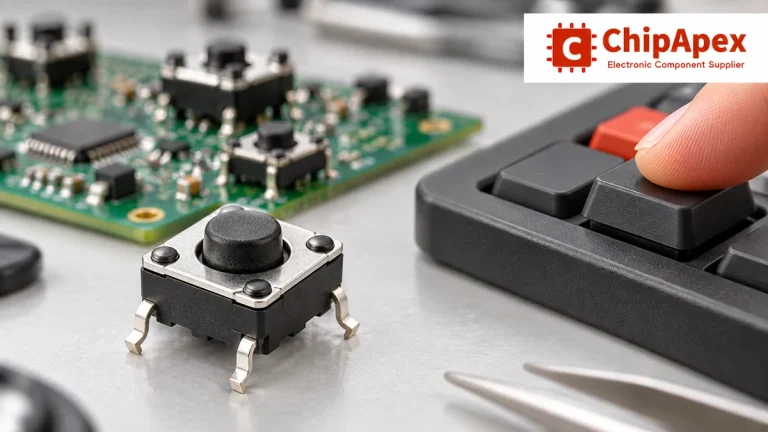
Choose tactile switches by operating force, travel, actuator height, footprint and lifetime. Check debounce, sealing and the assembled button mechanism.
Read More
XCVU9P-2FLGC2104E is listed in the Field Programmable Gate Array range at ChipApex. The manufacturer field lists AMD. Its product description is IC FPGA 416…
Read More
XCVU9P-2FLGC2104E is listed in the Field Programmable Gate Array range at ChipApex. The manufacturer field lists AMD. Its product description is IC FPGA 416…
Read More
XCVU9P-2FLGC2104E is listed in the Field Programmable Gate Array range at ChipApex. The manufacturer field lists AMD. Its product description is IC FPGA 416…
Read More
XCVU9P-2FLGC2104E is listed in the Field Programmable Gate Array range at ChipApex. The manufacturer field lists AMD. Its product description is IC FPGA 416…
Read More
XCVU9P-2FLGC2104E is listed in the Field Programmable Gate Array range at ChipApex. The manufacturer field lists AMD. Its product description is IC FPGA 416…
Read More
XCVU9P-2FLGC2104E is listed in the Field Programmable Gate Array range at ChipApex. The manufacturer field lists AMD. Its product description is IC FPGA 416…
Read More
XCVU9P-2FLGC2104E is listed in the Field Programmable Gate Array range at ChipApex. The manufacturer field lists AMD. Its product description is IC FPGA 416…
Read More
XCVU9P-2FLGC2104E is listed in the Field Programmable Gate Array range at ChipApex. The manufacturer field lists AMD. Its product description is IC FPGA 416…
Read More
Compare RC, crystal and MEMS oscillator circuits. Check ppm, jitter, load capacitance, startup margin and output compatibility before choosing a clock source.
Read More
XCVU9P-2FLGC2104E is listed in the Field Programmable Gate Array range at ChipApex. The manufacturer field lists AMD. Its product description is IC FPGA 416…
Read More
The activity of extra discounts on wholesale prices is in full swing…
Please fill in your contact information and we will send you the latest wholesale price list.






