 ChipApex | Global Electronic Components Supplier

SEARCH
Search Product
Search Post
— IC芯片 | 连接器 | 传感器 | 被动器件 —
Search productSearch post
— IC芯片 | 连接器 | 传感器 | 被动器件 —
The trend of science and technology is changing rapidly.
A radio frequency detector converts an RF input into a lower-frequency signal that represents a property such as signal envelope or power level. In electronic equipment, it supports transmit-power control, signal monitoring and measurement. Its frequency range, response type and calibration determine what the output can tell you.
The phrase also describes complete handheld instruments used to locate radio transmissions. Those instruments combine an antenna, RF circuitry, processing and a display or alert. This guide focuses on the detector components within a measurement chain and the requirements needed to choose them.
A detector receives a controlled sample of an RF path. Depending on the application, a coupler, attenuator or other input network establishes a suitable signal level. The detector produces an output that can be filtered, digitized and interpreted using calibration data.
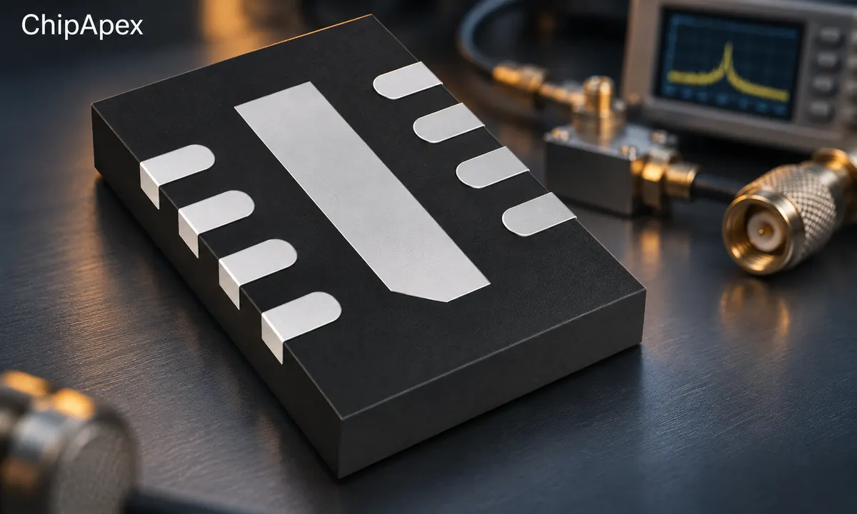
The input network belongs in the measurement model. If a coupler and cable introduce loss, the detector sees a different level from the original signal path. Frequency-dependent loss, mismatch and temperature can all change the relationship. The rf detector should be selected after defining that complete path.
A scalar detector measures a magnitude-related quantity. Identifying an unknown transmitter, decoding a protocol or distinguishing two simultaneous signals usually requires additional circuitry and analysis. An RF indication alone cannot establish which device produced the field.
Detector descriptions use two different ideas. Envelope and RMS describe what is being measured. A linear or logarithmic transfer characteristic describes how that measurement appears at the output. An RMS detector can therefore have a logarithmic output.
| Characteristic | What it provides | Selection consideration |
|---|---|---|
| Envelope detection | Output follows amplitude variations within its bandwidth | Modulation bandwidth and transient behavior |
| Logarithmic response | Approximately equal voltage changes for equal dB steps | Slope, intercept and log-conformance error |
| RMS response | Output represents an RMS-related measurement over defined conditions | Waveform bandwidth, averaging and crest-factor limits |
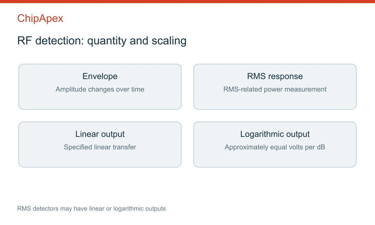
A detector calibrated with a continuous sine wave may produce a different error with a varying-envelope signal. Evaluate the waveform expected in service, including bursts and high peak-to-average ratios. The manufacturer's RF detector discussion explains the distinction between response types and output scaling.
For an envelope measurement, the output bandwidth must preserve the required changes. For average-power monitoring, filtering can reduce ripple, but it also increases settling time. Define whether the result needs to follow a short burst, a slow power adjustment or a long-term average.
Frequency coverage must include the actual band and the behavior of the input network. A headline upper frequency does not establish accuracy at every frequency below it. Coupling capacitors and matching components can also set a lower operating limit.
Specify minimum and maximum input power at the detector, including tolerances and faults. Distinguish the calibrated measurement range from the absolute maximum input. A device may survive a level at which its output is already inaccurate or saturated.
The low-frequency detector application note shows how external circuitry and detector architecture affect operation. Use the selected model's specified conditions when extending a design into another frequency band.
An input attenuator can protect the measurement range, but it also lowers sensitivity to weak signals. Its loss and tolerance become part of the calibration. For a changing rf signal, also check whether the detector must handle several bands or power states without a hardware change.
dBm expresses power relative to 1 mW. A 0 dBm signal is 1 mW, while 10 dBm is 10 mW. Conversion from power to voltage requires the relevant impedance and waveform conditions. An RF power value does not imply a universal voltage at every input.
For a hypothetical logarithmic detector with a slope of 25 mV/dB, a 10 dB input change produces a 250 mV output change within its calibrated region. The slope alone cannot determine absolute power. An intercept or equivalent calibration relationship is also needed.
Real calibration may use several power points and frequencies. Temperature compensation and residual nonlinearity can remain after calibration. Record the source accuracy, attenuator loss and measurement uncertainty so that a clean-looking output is not mistaken for a complete accuracy result.
If an adc converter reads the output, compare its range, resolution and acquisition behavior with the detector's slope and output drive. An illustrative 1 mV voltage uncertainty corresponds to 0.04 dB with a 25 mV/dB slope. Detector error and RF-path uncertainty remain separate contributions.
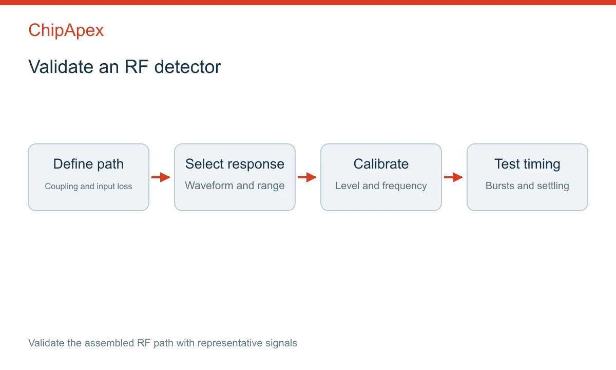
Check rise time, fall time, settling and recovery from overload. These conditions can differ from the small-signal output bandwidth. A burst detector may need to capture a level before the RF event ends, while a power-control loop needs a stable response over its operating range.
An output capacitor can reduce noise or average the response, but the permitted value and resulting dynamics are device-specific. Verify interaction with the ADC input and any additional buffer. A suitable voltage reference may be relevant to the ADC's scale accuracy where the converter uses an external reference.
Follow the RF layout requirements for input impedance, ground connections and supply decoupling. PCB coupling can create an apparent response even when the intended input path is disconnected. Evaluate the assembled board with representative supplies, cables and RF levels.
Send ChipApex the preferred part number, frequency band, input-power range, waveform, required response type, timing, supply, output interface, package and quantity. Include the measurement target in dB or another clearly defined unit and identify the expected temperature range.
For replacements, compare the transfer function, pinout and calibration requirements. A different slope or response architecture may require firmware or circuit changes even if the new device fits the same board area.
A power or envelope detector generally provides an amplitude-related output over its operating band. Measuring the frequency requires an appropriate frequency-selective or counting architecture. A complete instrument may combine several functions, so check what its displayed value actually represents.
No. Logarithmic describes the output scaling. The underlying measurement may respond to an envelope or to an RMS-related quantity. Check the architecture and waveform-dependent accuracy because a logarithmic output by itself does not establish RMS behavior.
Detection depends on transmission activity, frequency, signal strength, antenna coupling and the receiver design. A silent device may produce no useful RF indication. Even an active signal requires further investigation to identify its source. Component sensitivity alone cannot establish complete instrument performance.
Different waveform envelopes and peak-to-average ratios can affect the detector response. Averaging, bandwidth and crest-factor limits also matter. Calibrate and test using a waveform representative of the intended application, with input levels kept inside the specified measurement range.
Only with the appropriate calibrated transfer relationship and input-path corrections. The detector's frequency, supply, temperature and output-loading conditions must be accounted for. A voltage value without that context cannot reliably establish the original RF power.
Understand voltage controlled oscillator tuning, phase noise and PLL operation. Check supply noise, output loading and requirements before selection.
View details
Select a bridge rectifier by reverse voltage, capacitor charging current, startup surge and cooling. Work through a stated DC voltage and ripple example.
View details
Understand tactile switches, PCB and keyboard differences, four-pin wiring, debounce, force, travel and replacement checks for reliable control inputs.
View details
Practical MCU selection guide for engineers: compare STM32, ESP32 & NXP, avoid counterfeits, and ensure supply chain reliability. Authored by ChipApex FAE.
View details
The activity of extra discounts on wholesale prices is in full swing…
Please fill in your contact information and we will send you the latest wholesale price list.

