 ChipApex | Global Electronic Components Supplier

SEARCH
Search Product
Search Post
— IC芯片 | 连接器 | 传感器 | 被动器件 —
Search productSearch post
— IC芯片 | 连接器 | 传感器 | 被动器件 —
The trend of science and technology is changing rapidly.
An analog front end, or AFE, prepares a real-world electrical signal for conversion or further processing. It may provide amplification, filtering, biasing, protection, excitation and conversion, depending on the device. Its purpose is to deliver a usable signal without losing the information the system needs.
An analog front end is not always a single integrated circuit, and not every AFE includes an ADC. Read the functional block diagram before comparing parts. A highly integrated device can simplify a design, but only when its input architecture and operating limits fit the sensor.
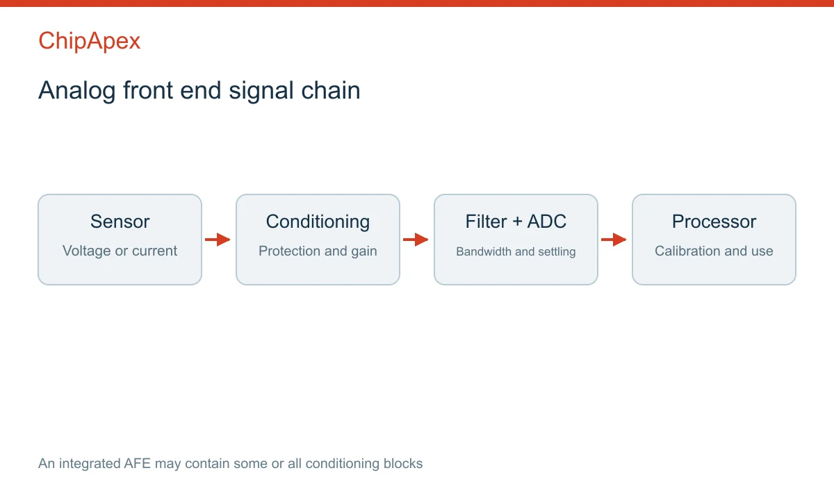
A typical measurement path starts with a sensor, passes through protection and conditioning, then reaches an ADC and digital processor. The AFE may cover several of these blocks. A photodiode interface may need a transimpedance amplifier; a bridge sensor may need differential gain; an electrode interface may require extremely low input current.
The sensor defines the starting conditions: output type, amplitude, impedance, bandwidth, common-mode voltage and fault exposure. Those conditions should be written down before selecting gain or resolution. A voltage-output sensor and a current-output sensor may require entirely different input stages even if both measure the same physical quantity.
For a discrete implementation, compare the input stage with the available instrumentation op amp options. An integrated AFE may offer matched channels, programmable gain and excitation, while a discrete design can provide more freedom over voltage range and component choice.
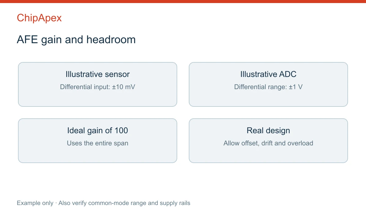
Gain should use the converter's input range effectively while preserving headroom. Include the sensor's maximum useful output, offset, tolerance, temperature drift and overload recovery. A signal that fits at room temperature may clip at a production or environmental extreme.
Consider an idealized differential signal spanning ±10 mV and an ADC accepting ±1 V differential. A gain of 100 reaches the full input span exactly, leaving no allowance for offset or excess signal. A lower gain may produce a more reliable measurement once real tolerances are included. This calculation does not establish valid supply rails or input common-mode conditions.
The amplifier's input common-mode range and output swing are separate constraints. A small differential voltage can sit on a common-mode voltage that the amplifier cannot accept. Likewise, an ADC's differential range does not mean either input can move freely outside its absolute or specified operating limits.
Programmable gain can help when the signal range changes, but gain changes may require a settling interval. Evaluate accuracy and noise at every gain setting actually used, rather than relying on the best number in the headline specification.
Noise and accuracy are not interchangeable. Random noise limits repeatability; offset, gain error, reference error and drift can shift the result systematically. Calibration can correct some stable errors, but it does not remove all noise, temperature effects or nonlinear behavior.
| Contributor | Why it matters | Useful check |
|---|---|---|
| Input voltage noise | Adds uncertainty to small signals | Integrate over the measurement bandwidth |
| Input current noise | Creates voltage noise through source impedance | Evaluate the actual sensor impedance |
| Offset and drift | Shift readings and change with temperature | Budget before and after calibration |
| Reference error | Changes converter scale | Include reference noise and drift |
| Interference | May alias or overload the input | Test realistic wiring and environment |
Specify bandwidth before comparing noise figures. A noise density at one frequency is not the total noise in the measurement. Low-frequency noise can be important in slow measurements, while wider bandwidth admits more broadband noise.
The voltage reference deserves its own budget. In some systems, ratiometric measurement reduces sensitivity to excitation variation; in others, absolute reference performance is central to accuracy. The appropriate approach depends on the sensor and converter architecture.
An anti-alias filter reduces unwanted frequency content before sampling. A digital filter after conversion cannot recover information already corrupted by aliasing. Filter order, cutoff and phase response should follow the signal bandwidth and rejection requirement.
The ADC input may also present a switched-capacitor load. The driver and local RC network must settle sufficiently during the acquisition interval. A filter that looks suitable from its cutoff frequency alone can still cause settling error if its source impedance is too high for the selected sampling conditions.
When comparing an adc converter, check input structure, acquisition time, reference drive and multiplexing behavior. Switching channels can introduce charge redistribution and large steps, so performance on a steady input does not prove performance in a scanning system.
Manufacturer analog circuit design resources provide practical amplifier and converter interface examples. Treat example circuits as starting points and recalculate their operating conditions for your sensor.
An integrated AFE may reduce component count and provide useful calibration or diagnostic functions. A discrete implementation may better accommodate unusual input voltages, specialized protection or a particular noise target. Compare the complete system, including power, firmware, layout and component availability.
Validate the design with minimum and maximum inputs, common-mode extremes, expected temperature range and representative interference. Check overload recovery as well as normal operation. On a multichannel board, test crosstalk with one channel driven strongly while another measures a small signal.
For a ChipApex sourcing request, provide sensor type, input range, channel count, bandwidth, supply rails, interface, package and target quantity. Include the preferred part number and acceptable alternatives. These details allow the sourcing discussion to focus on a suitable architecture rather than an AFE label alone.
No. An ADC converts an analog signal to digital data. An AFE conditions the signal and may include an ADC as one of several functions.
No. Gain can use more of the ADC range, but it can also amplify offsets, increase clipping risk and change bandwidth or settling behavior. The input-referred system noise remains important.
Software can compensate for some characterized errors. It cannot restore a clipped signal or reliably remove information loss caused by aliasing and inadequate settling.
It is useful when a differential signal requires gain with high input impedance and common-mode rejection. Check the actual common-mode range and source conditions for the selected part.
No. Sensor output type, impedance, signal range and bandwidth determine the required architecture. Shared digital interfaces do not imply interchangeable analog inputs.
Choose a rocker switch by AC/DC ratings, contact arrangement, illumination, panel fit and sealing. Get practical checks for engineering and component sourcing.
View details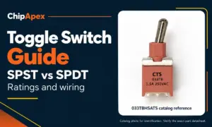
Compare SPST and SPDT toggle switches, understand AC/DC ratings, and follow wiring examples. Check contact action, mounting and parts in the ChipApex catalog.
View details
Choose LED drivers by current, string voltage, dimming and thermal limits. Understand constant-current operation and the checks needed for your load.
View details
Practical MCU selection guide for engineers: compare STM32, ESP32 & NXP, avoid counterfeits, and ensure supply chain reliability. Authored by ChipApex FAE.
View details
The activity of extra discounts on wholesale prices is in full swing…
Please fill in your contact information and we will send you the latest wholesale price list.

