 ChipApex | Global Electronic Components Supplier

SEARCH
Search Product
Search Post
— IC芯片 | 连接器 | 传感器 | 被动器件 —
Search productSearch post
— IC芯片 | 连接器 | 传感器 | 被动器件 —
The trend of science and technology is changing rapidly.
Use a ferrite bead by placing it in a suitable current path where its frequency-dependent impedance can reduce unwanted high-frequency noise. Select it from impedance curves at the noise frequency and operating current, then validate the complete circuit. A bead chosen only by its impedance at 100 MHz may provide little benefit where the actual problem occurs.
For a PCB supply branch, ferrite beads are often combined with local capacitors. The combination can attenuate noise, but it can also create resonance or excessive voltage drop. Placement and measurement are part of the design, not optional finishing steps.
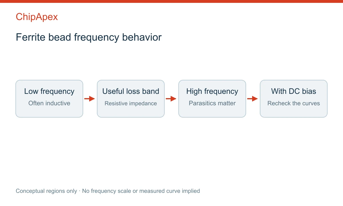
A bead has resistive and reactive impedance components. At lower frequencies it may behave mainly inductively. Over a useful higher-frequency region, its resistive component can dissipate noise energy. At still higher frequencies, parasitic effects change the response again.
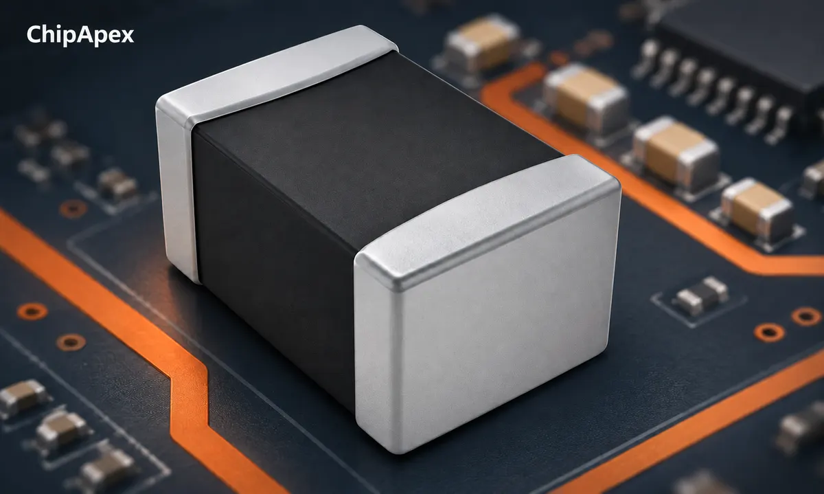
The headline impedance is the magnitude at a specified frequency and test condition. It does not show how much of that impedance is resistive, how the part behaves elsewhere, or what happens under DC bias. Compare the manufacturer's R, X and Z curves when available.
A bead is not interchangeable with every inductor. Power inductors are commonly selected to store energy in converters, while suppression beads are selected for their noise impedance and loss behavior. The intended function and frequency response decide which component belongs in the circuit.
Establish whether the problem is conducted or radiated, and whether the relevant current is differential-mode or common-mode. A bead in one supply conductor does not address every coupling path. Noise may bypass it through ground, a cable shield, parasitic capacitance or another supply branch.
A PCB chip bead in a supply rail and a clamp-on ferrite around a complete cable also operate in different circuit contexts. When forward and return conductors pass through the same core, their normal differential currents can largely cancel magnetically while common-mode current sees impedance. That is different from placing a chip bead in series with only one conductor.
For a cable common-mode problem, compare the requirements with common mode chokes or a suitable cable ferrite. Choose the solution from the measured noise path rather than from package convenience.
Record the troublesome frequency range, load current, supply tolerance and permitted transient response. These measurements make the first component selection much more useful than trying a random bead and judging only whether one oscilloscope trace looks smoother.
| Parameter | What to check |
|---|---|
| Impedance versus frequency | Useful impedance where the unwanted noise exists |
| Resistance and reactance | Whether attenuation relies on loss or a reactive network |
| DC bias behavior | Impedance at the actual operating current |
| DC resistance | Supply drop and continuous dissipation |
| Current and temperature rating | Thermal limits under the board's conditions |
| Package and parasitics | Layout fit and high-frequency behavior |
DC bias can substantially reduce the bead's effective impedance. A current rating may primarily describe temperature rise or another manufacturer limit; it does not promise that the zero-bias impedance curve remains valid up to that current.
For an illustrative bead with 50 mΩ DC resistance carrying 1 A, the DC drop is 50 mV and dissipation is 50 mW. At 2 A, the drop becomes 100 mV and dissipation 200 mW, before considering temperature dependence. The actual part must meet both electrical and thermal requirements.
The manufacturer's ferrite bead application note discusses DC bias and unwanted resonance. Its examples explain the mechanisms; their numerical results should not be transferred to an unrelated bead or PCB.
For a filtered supply branch, the local decoupling capacitor is commonly placed on the load side with a short return path. The bead, capacitor, source impedance and load impedance form one network. Long traces and poor return geometry can undermine its intended behavior.
Do not casually insert a bead in a signal reference or ground return. Added impedance can disturb reference levels or force current through unintended paths. Follow the IC's layout guidance, especially for mixed-signal devices where a continuous reference plane may be important.
If the filtered branch supplies an analog front end, check both steady noise and supply transients during mode changes or channel activity. The bead must not starve the circuit of transient current or create a disturbance that appears as a measurement error.
A bead and low-ESR capacitor can form an underdamped network with a resonant peak. Instead of attenuating a particular disturbance, the network may amplify it near resonance. Source and load impedance, capacitor ESR and bead loss all affect the result.
Damping may involve a different bead, a deliberate resistive path, an RC branch or a different capacitor arrangement. Each option has consequences for power, voltage drop and attenuation. Use an appropriate model and measurements to select the approach rather than copying a universal component value.
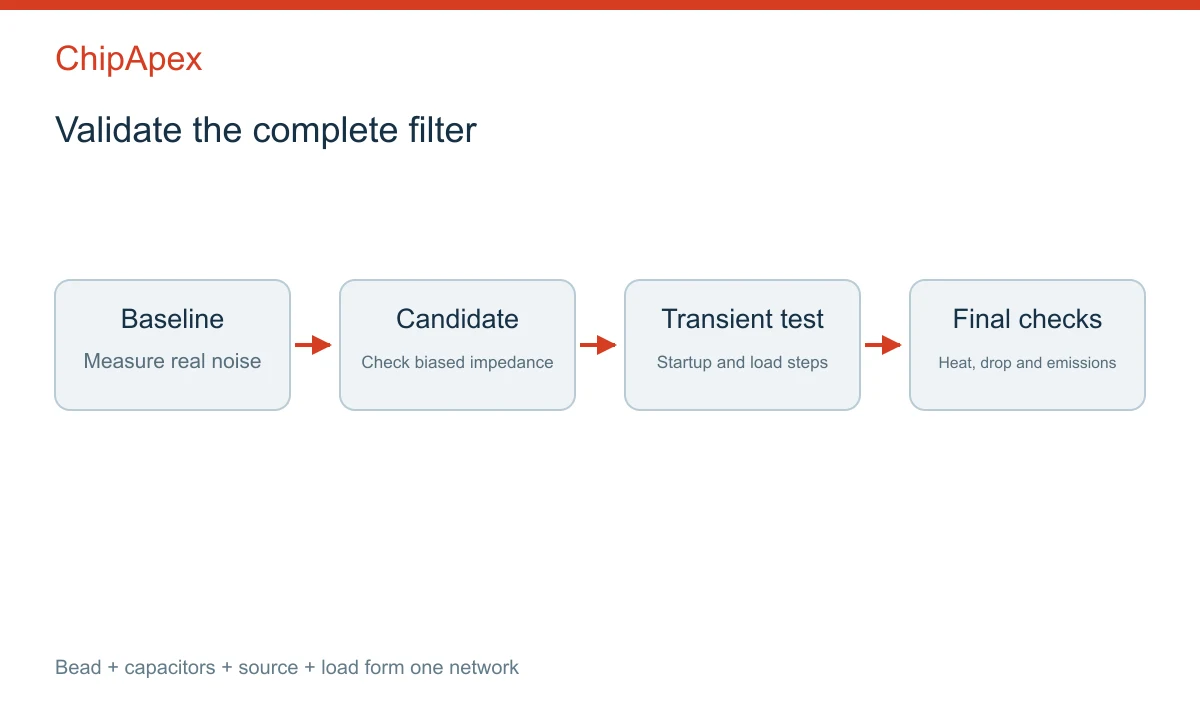
Test startup and load steps as well as a steady operating condition. A quiet steady-state rail can still overshoot or droop during a transient. Check regulator stability and feedback placement if the filter is near a regulated supply output.
Measure a baseline, install the candidate network, and repeat the measurement with the same probe setup, load and bandwidth. A long probe ground lead can create misleading high-frequency artifacts. For emissions work, confirm the result with the relevant test setup rather than relying on a single near-field or scope observation.
Evaluate several operating points, including the highest intended current and representative temperature. Confirm that the improvement persists and that the bead does not introduce excessive heat, supply drop or transient ringing.
Send ChipApex the preferred ferrite bead part number, target noise band, current, maximum DC resistance, package and quantity. Ask for impedance curves and DC-bias information when considering alternatives. A matching “600 Ω at 100 MHz” label alone does not establish equivalent performance.
No. Add one when a defined noise problem and a validated filter design justify it. Unnecessary filtering can introduce voltage drop or resonance.
No. The impedance must occur in the useful frequency range and remain suitable under bias. Its interaction with the source, load and capacitors also matters.
Many suppression beads have little impedance at low ripple frequencies. Another filter topology or a change to the supply design may be needed.
Possible causes include resonance, a changed return path, inadequate decoupling or a measurement artifact. Compare the complete network and probe setup with the baseline.
It may preserve DC continuity, but it removes the intended noise impedance. Use such a change only as a controlled diagnostic or after validating the system without the bead.
Learn how a JFET works and how to compare bias, leakage, noise and pinout. Review practical selection questions for high-impedance analog circuits.
View details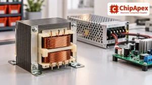
Select power transformers by input frequency, secondary VA, rectifier load, isolation, regulation and inrush. Build a clearer specification for your next RFQ.
View details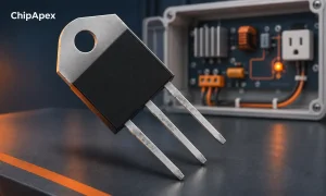
Learn how a TRIAC switches AC loads. Understand triggering, latching, holding current, phase control and thermal limits before choosing a component.
View details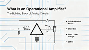
Stop guessing which Op-Amp to use. We break down GBWP, Slew Rate, and Offset Voltage with real engineering insights. Find the right parts like NE5532DR & LM358DR at ChipApex.
View details
The activity of extra discounts on wholesale prices is in full swing…
Please fill in your contact information and we will send you the latest wholesale price list.

