 ChipApex | Global Electronic Components Supplier
71V2556S100PFG
Search Product
Search Post
— IC芯片 | 连接器 | 传感器 | 被动器件 —
Search productSearch post
— IC芯片 | 连接器 | 传感器 | 被动器件 —
Consult the customer manager about the wholesale price.
consultation hotline:86-132-6715-2157
email:[email protected]
Contact the product manager for consultation. One-stop consultation is available.
Do you want a lower wholesale price? Please send us your inquiry and we will reply immediately.
The 71V2556S100PFG is a 4.5 Mbit synchronous static random-access memory (SRAM) integrated circuit manufactured by Renesas Electronics Corporation. It features a parallel interface with a data organization of 128K x 36 bits. The device operates at a maximum clock frequency of 100 MHz and provides an access time of 5 ns. It requires a supply voltage range of 3.135 V to 3.465 V. The component is housed in a 100-pin Thin Quad Flat Package (TQFP) with dimensions of 14x14 mm. It supports an industrial operating temperature range from -40°C to +85°C.
Verify RoHS compliance status as documentation indicates variations across production lots; some sources list compliance while others note non-compliance. Confirm package marking and date codes against current manufacturing notices. Check for End-of-Life declarations affecting long-term availability. Validate moisture sensitivity level handling procedures during assembly.
Select this component when ZBT performance is required to maximize bus throughput without turnaround latency. Ensure system design accommodates the specific 3.3V core voltage and 2.5V I/O voltage requirements. Verify that the 100-pin TQFP footprint matches the PCB layout constraints. Consider thermal dissipation capabilities within the specified industrial temperature range.
This part belongs to the 71V2556 family of synchronous SRAMs, which utilizes Zero Bus Turnaround technology to enhance data transfer efficiency. The family includes variants with different speeds and packages, such as the 71V2556S150PFGI for higher speed applications. The 71V2556 series is designed for applications requiring high-density memory with fast access times in a compact surface-mount package.
The 71V2556S133PFG offers similar functionality with a higher clock frequency of 133 MHz. The 71V2556S150PFGI provides increased speed up to 150 MHz. Both alternatives maintain the same 128K x 36 organization and 100-pin TQFP package, ensuring pin compatibility.
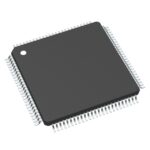 71V2556S100PFG
The activity of extra discounts on wholesale prices is in full swing…
Please fill in your contact information and we will send you the latest wholesale price list.





