 ChipApex | Global Electronic Components Supplier

SEARCH
Search Product
Search Post
— IC芯片 | 连接器 | 传感器 | 被动器件 —
Search productSearch post
— IC芯片 | 连接器 | 传感器 | 被动器件 —
Consult the customer manager about the wholesale price.
consultation hotline:86-132-6715-2157
email:[email protected]
Contact the product manager for consultation. One-stop consultation is available.
Do you want a lower wholesale price? Please send us your inquiry and we will reply immediately.
74LVC157ADB-Q100J is listed in the Signal Switches, Multiplexers, Decoders range at ChipApex. The manufacturer field lists Nexperia USA Inc.. Its product description is IC MULTIPLEXER 4 X 2:1 16SSOP. Review the specifications below when checking this part for your BOM.
The Nexperia 74LVC157ADB-Q100J is a quad 2-input multiplexer qualified to AEC-Q100 Grade 1 standards. It operates with a supply voltage range of 1.2 V to 3.6 V and features 5 V tolerant inputs for interfacing with 5 V logic. The device includes an active LOW enable input (E) that forces outputs LOW when HIGH, and a common select input (S) determining the data source. It supports mixed 3.3 V and 5 V applications and provides ESD protection exceeding 2000 V (HBM) and 1000 V (CDM).
Verify the exact package type against the ordering code, as the base part number covers multiple packages. Confirm the suffix 'J' corresponds to the specific tape and reel configuration required for your assembly line. Ensure the design accounts for the -40 °C to +125 °C operating temperature range specified for automotive reliability.
Select this component for designs requiring robust automotive-grade multiplexing with wide voltage tolerance. The 5 V tolerant inputs simplify integration into legacy 5 V systems while supporting modern lower voltage logic. Consider the available package options if space constraints exist, noting that the AD variant refers to the SO16 package family within the broader product line.
This device belongs to the 74LVC157A-Q100 series of quad multiplexers designed for automotive electronics. The series ensures high reliability and performance across extreme temperature ranges. It serves as a standard solution for signal routing and data selection in complex vehicle electronic architectures where voltage translation and noise immunity are critical.
The datasheet revision history indicates that the specific type number 74LVC157ADB-Q100 was removed in version 3. Designers should verify current availability and potential pin-compatible alternatives within the 74LVC157A-Q100 family, such as the APW or ABQ variants, depending on the required package style.
The enable input (E) is active LOW. When pin E is HIGH, all outputs (1Y to 4Y) are forced LOW regardless of other input conditions.
Yes, the device features 5 V tolerant inputs, allowing it to be driven by 5 V devices and used as a translator in mixed 3.3 V and 5 V applications.
Explore related parts through Logic, Integrated Circuits (ICs), all product categories, ChipApex homepage.
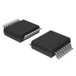 74LVC157ADB-Q100J

74LVC157ADB-Q100J is listed in the Signal Switches, Multiplexers, Decoders range at ChipApex. The manufacturer field lists Nexperia USA Inc.. Its product description is IC…
Read More
74LVC157ADB-Q100J is listed in the Signal Switches, Multiplexers, Decoders range at ChipApex. The manufacturer field lists Nexperia USA Inc.. Its product description is IC…
Read More
74LVC157ADB-Q100J is listed in the Signal Switches, Multiplexers, Decoders range at ChipApex. The manufacturer field lists Nexperia USA Inc.. Its product description is IC…
Read More
74LVC157ADB-Q100J is listed in the Signal Switches, Multiplexers, Decoders range at ChipApex. The manufacturer field lists Nexperia USA Inc.. Its product description is IC…
Read More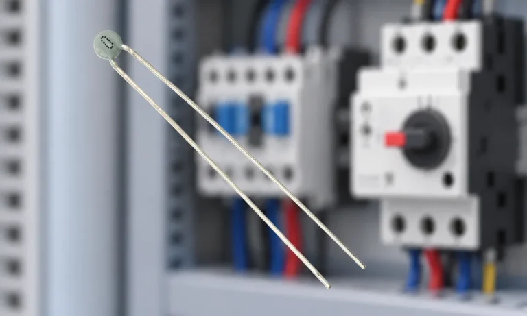
Learn why PTC resistance rises with temperature, how it differs from NTC, and which ratings matter for sensing and protection.
Read More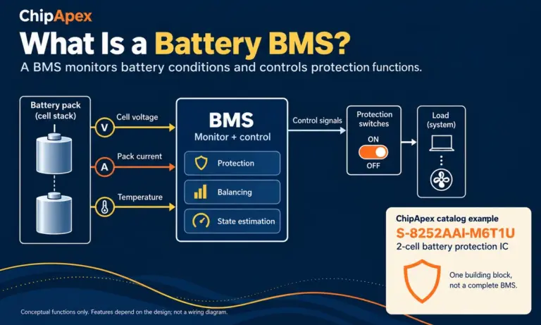
Learn what a battery BMS does, how protection differs from charging, and which pack specifications to check when sourcing BMS components through ChipApex.
Read More
74LVC157ADB-Q100J is listed in the Signal Switches, Multiplexers, Decoders range at ChipApex. The manufacturer field lists Nexperia USA Inc.. Its product description is IC…
Read More
74LVC157ADB-Q100J is listed in the Signal Switches, Multiplexers, Decoders range at ChipApex. The manufacturer field lists Nexperia USA Inc.. Its product description is IC…
Read More
74LVC157ADB-Q100J is listed in the Signal Switches, Multiplexers, Decoders range at ChipApex. The manufacturer field lists Nexperia USA Inc.. Its product description is IC…
Read More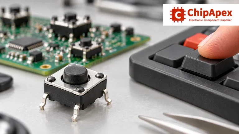
Understand tactile switches, PCB and keyboard differences, four-pin wiring, debounce, force, travel and replacement checks for reliable control inputs.
Read More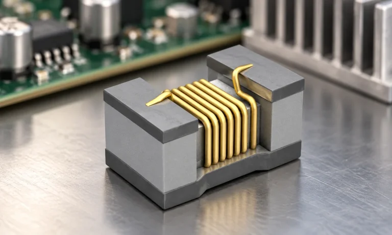
See when an inductor behaves linearly, how DC bias and saturation reduce inductance, and which current and temperature curves to check.
Read More
74LVC157ADB-Q100J is listed in the Signal Switches, Multiplexers, Decoders range at ChipApex. The manufacturer field lists Nexperia USA Inc.. Its product description is IC…
Read More
The activity of extra discounts on wholesale prices is in full swing…
Please fill in your contact information and we will send you the latest wholesale price list.





