 ChipApex | Global Electronic Components Supplier
9DBL0252BKILF
Search Product
Search Post
— IC芯片 | 连接器 | 传感器 | 被动器件 —
Search productSearch post
— IC芯片 | 连接器 | 传感器 | 被动器件 —
Consult the customer manager about the wholesale price.
consultation hotline:86-132-6715-2157
email:[email protected]
Contact the product manager for consultation. One-stop consultation is available.
Do you want a lower wholesale price? Please send us your inquiry and we will reply immediately.
The 9DBL0252BKILF is a 3.3V PCIe Zero-Delay Buffer manufactured by Integrated Device Technology, now part of Renesas Electronics Corporation. It provides two low-skew output clocks derived from a single input, designed to eliminate clock skew in high-speed serial interfaces. The device utilizes a Phase-Locked Loop (PLL) architecture to maintain zero input-to-output delay while ensuring signal integrity for PCI Express applications. It operates within a standard industrial temperature range and is packaged in a lead-free, RoHS-compliant format suitable for surface-mount assembly.
Verify the manufacturer designation carefully, as this component was originally produced by Integrated Device Technology (IDT). Following IDT's acquisition by Renesas Electronics, supply chain documentation may reflect either entity. Confirm the specific package variant and temperature grade against current datasheets to ensure compatibility with existing board designs.
Select this component when a dual-channel zero-delay buffering solution is required for 3.3V logic families. Ensure the design supports the necessary PLL loop bandwidth for the target application's jitter requirements. Compare against higher-output variants like the 9DBL04 or 9DBL06 if additional clock lanes are needed later in the design cycle.
This part belongs to the 9DBL series of zero-delay buffers, which are widely used in networking and computing platforms. The 'BK' suffix typically denotes a specific package type and pinout configuration distinct from other members of the family. These devices serve as critical timing elements in systems where clock domain synchronization is mandatory for data integrity.
Direct replacements include the 9DBL0252BKILFT (tape and reel version) or the generic 9DBL0242. Cross-voltage alternatives such as the 2305 series require level shifting considerations. Verify pin-to-pin compatibility before substituting with other manufacturers' PCIe buffers.
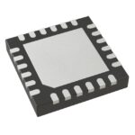 9DBL0252BKILF
The activity of extra discounts on wholesale prices is in full swing…
Please fill in your contact information and we will send you the latest wholesale price list.






