ChipApex | Global Electronic Components Supplier
9FGV1006A004LTGI8
Search Product
Search Post
— IC芯片 | 连接器 | 传感器 | 被动器件 —
Search productSearch post
— IC芯片 | 连接器 | 传感器 | 被动器件 —
Consult the customer manager about the wholesale price.
consultation hotline:86-132-6715-2157
email:[email protected]
Contact the product manager for consultation. One-stop consultation is available.
Do you want a lower wholesale price? Please send us your inquiry and we will reply immediately.
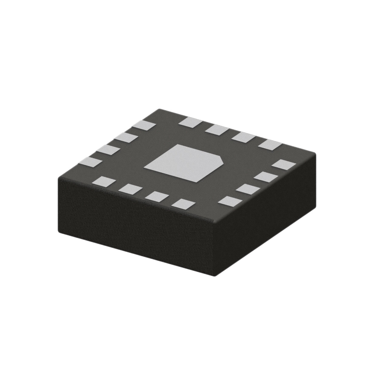
The 9FGV1006A004LTGI8 is a programmable clock generator IC from Renesas' PhiClock™ family. It operates with a single supply voltage ranging from 1.71V to 3.465V and supports input frequencies via HCSL, LVCMOS, LVDS, or crystal sources. The device features one circuit with a 1:4 input-to-output ratio, delivering outputs in HCSL, LVCMOS, LVDS, and LVPECL formats. It achieves a maximum frequency of 325MHz and includes integrated PLL functionality for frequency synthesis. Designed for surface mount installation, it utilizes a 16-TFLGA package with an exposed pad, suitable for applications requiring precise timing signals within a -40°C to 85°C operating temperature range.
Verify the specific suffix 'A004' against official Renesas documentation to confirm factory-configured parameters, as this series consists of factory-programmable devices. Ensure compatibility with the 16-TFLGA exposed pad thermal requirements during PCB layout. Confirm RoHS3 compliance status through current datasheets, as manufacturing processes may evolve. Cross-reference the part number with authorized distributors to validate authenticity and traceability.
Select this component when a 1:4 clock fan-out with mixed signaling standards is required. The 16-TFLGA package offers a compact footprint for space-constrained designs. Verify that the target application's voltage domain aligns with the 1.71V–3.465V supply range. Consider the 325MHz maximum frequency limit relative to downstream component requirements. Evaluate thermal dissipation needs due to the exposed pad design in high-density layouts.
This device belongs to the Renesas PhiClock™ programmable clock generator family, which provides flexible timing solutions for high-performance digital systems. The 9FGV1006 variant specifically addresses applications needing four synchronized output clocks derived from a single input source. It complements other members like the 9FGV1004 and 9FGV1008 by offering a specific pin count and output configuration optimized for mid-range clock distribution tasks.
Direct substitutes within the same family include the 9FGV1006Q550LTGI8, though verification of electrical characteristics and pinout compatibility is essential. Generic clock generators may require significant redesign of power and signal integrity layers. Always consult the latest datasheet addendums for any pin-compatible alternatives recommended by Renesas.
 9FGV1006A004LTGI8
The activity of extra discounts on wholesale prices is in full swing…
Please fill in your contact information and we will send you the latest wholesale price list.