ChipApex | Global Electronic Components Supplier

SEARCH
Search Product
Search Post
— IC芯片 | 连接器 | 传感器 | 被动器件 —
Search productSearch post
— IC芯片 | 连接器 | 传感器 | 被动器件 —
Consult the customer manager about the wholesale price.
consultation hotline:86-132-6715-2157
email:[email protected]
Contact the product manager for consultation. One-stop consultation is available.
Do you want a lower wholesale price? Please send us your inquiry and we will reply immediately.
ADADC71KD is listed in the Analog To Digital Converters (ADC) range at ChipApex. The manufacturer field lists Analog Devices Inc.. Its product description is IC ADC 16BIT SAR 32BBDIP. Review the specifications below when checking this part for your BOM.
The ADADC71KD is a high-resolution 16-bit hybrid analog-to-digital converter featuring an integrated reference, clock, and laser-trimmed thin-film components. It operates with ±15 V analog supplies and a +5 V digital supply, consuming 645 mW typically. The device provides parallel TTL-compatible outputs and supports input ranges including ±2.5 V, ±5 V, ±10 V, 0 to +5 V, 0 to +10 V, and 0 to +20 V. Maximum linearity error is ±0.003% of FSR, with conversion times of 35 μs typical (50 μs max) for 14-bit resolution. It guarantees no missing codes up to 14 bits within the 0°C to +70°C operating temperature range.
Verify the specific suffix KD against the ordering guide to confirm the ±0.003% linearity specification and commercial temperature range. Ensure the procurement source is authorized, as this is a legacy hybrid ceramic DIP component. Confirm package integrity upon receipt, as hermetic seals are critical for long-term reliability in precision applications.
Select the ADADC71KD when strict linearity requirements below ±0.003% FSR are necessary. Compare against the JD grade if higher tolerance is acceptable. Consider the short cycle feature if faster throughput is needed at reduced bit resolutions. Evaluate power supply constraints due to the requirement for dual ±15 V rails alongside the +5 V logic supply.
The ADADC71 series represents a high-performance hybrid ADC solution from Analog Devices, designed for applications demanding superior accuracy and stability. The KD variant specifically targets environments requiring tighter linearity specifications compared to the standard JD grade. Its design leverages monolithic DAC technology to minimize drift and ensure monotonic behavior across the specified temperature range.
No direct public substitute part numbers are documented for the ADADC71KD. Designers should evaluate modern SAR or Sigma-Delta ADCs that offer comparable resolution and interface compatibility, noting differences in packaging and supply voltage requirements.
Complementary two's complement (CTC) coding is obtained by using an inverter to complement the most significant bit (Pin 1).
The maximum conversion time for 14-bit resolution is 50 μs.
Yes, an external clock can be used to control slower conversion times by applying narrow negative-going pulses to the START CONVERT input.
Explore related parts through Data Acquisition, Integrated Circuits (ICs), all product categories, ChipApex homepage.
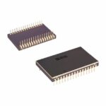 ADADC71KD
ADADC71KD is listed in the Analog To Digital Converters (ADC) range at ChipApex. The manufacturer field lists Analog Devices Inc.. Its product description is…
Read More
ADADC71KD is listed in the Analog To Digital Converters (ADC) range at ChipApex. The manufacturer field lists Analog Devices Inc.. Its product description is…
Read More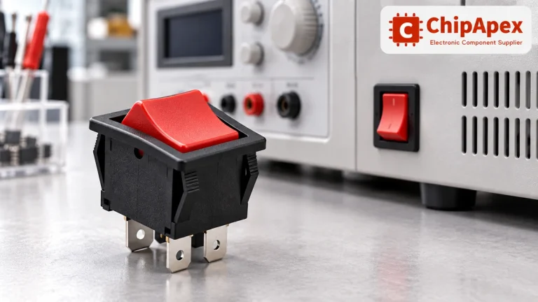
Choose a rocker switch by AC/DC ratings, contact arrangement, illumination, panel fit and sealing. Get practical checks for engineering and component sourcing.
Read More
ADADC71KD is listed in the Analog To Digital Converters (ADC) range at ChipApex. The manufacturer field lists Analog Devices Inc.. Its product description is…
Read More
ADADC71KD is listed in the Analog To Digital Converters (ADC) range at ChipApex. The manufacturer field lists Analog Devices Inc.. Its product description is…
Read More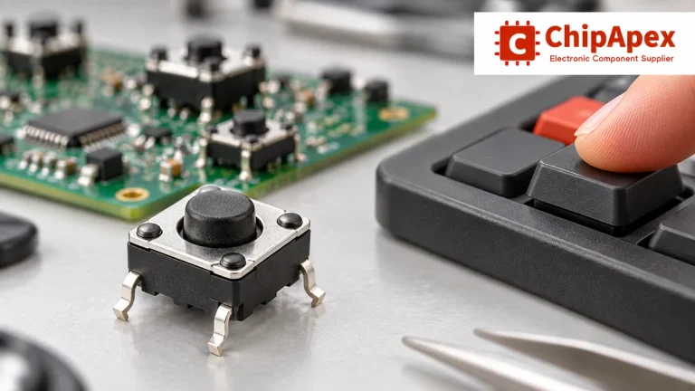
Choose tactile switches by operating force, travel, actuator height, footprint and lifetime. Check debounce, sealing and the assembled button mechanism.
Read More
ADADC71KD is listed in the Analog To Digital Converters (ADC) range at ChipApex. The manufacturer field lists Analog Devices Inc.. Its product description is…
Read More
ADADC71KD is listed in the Analog To Digital Converters (ADC) range at ChipApex. The manufacturer field lists Analog Devices Inc.. Its product description is…
Read More
ADADC71KD is listed in the Analog To Digital Converters (ADC) range at ChipApex. The manufacturer field lists Analog Devices Inc.. Its product description is…
Read More
ADADC71KD is listed in the Analog To Digital Converters (ADC) range at ChipApex. The manufacturer field lists Analog Devices Inc.. Its product description is…
Read More
ADADC71KD is listed in the Analog To Digital Converters (ADC) range at ChipApex. The manufacturer field lists Analog Devices Inc.. Its product description is…
Read More
ADADC71KD is listed in the Analog To Digital Converters (ADC) range at ChipApex. The manufacturer field lists Analog Devices Inc.. Its product description is…
Read More
The activity of extra discounts on wholesale prices is in full swing…
Please fill in your contact information and we will send you the latest wholesale price list.