 ChipApex | Global Electronic Components Supplier

SEARCH
Search Product
Search Post
— IC芯片 | 连接器 | 传感器 | 被动器件 —
Search productSearch post
— IC芯片 | 连接器 | 传感器 | 被动器件 —
Consult the customer manager about the wholesale price.
consultation hotline:86-132-6715-2157
email:[email protected]
Contact the product manager for consultation. One-stop consultation is available.
Do you want a lower wholesale price? Please send us your inquiry and we will reply immediately.
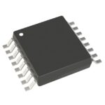
ADG661BRU is listed in the Analog Switches, Multiplexers, Demultiplexers range at ChipApex. The manufacturer field lists Analog Devices Inc.. Its product description is IC SWITCH QUAD SPST 16TSSOP. Review the specifications below when checking this part for your BOM.
The ADG661BRU is a monolithic CMOS device comprising four independently selectable SPST switches, fabricated using LC2MOS technology. It operates from +5 V single or ±5 V dual supplies with an analog signal range extending to the rails. Key electrical parameters include a maximum on-resistance of 75 Ω at +4.5 V single supply and 50 Ω at ±4.5 V dual supply. Leakage currents are typically ±0.025 nA (max ±2.5 nA). Switching times are 250 ns max (tON) and 45 ns max (tOFF) under single supply conditions. The device features low charge injection of 12 pC typical and operates within a temperature range of –40 °C to +85 °C.
Verify the specific suffix RU-16 corresponds to the 16-lead TSSOP package when sourcing. Confirm that the B version designation aligns with the industrial temperature range of –40 °C to +85 °C. Ensure compatibility with existing PCB footprints for the TSSOP-16 form factor during component replacement or new design integration.
Select the ADG661BRU for applications requiring low distortion and wide signal bandwidth due to its flat Ron profile. Choose this part over inverted logic variants (ADG662) if standard active-low control inputs are preferred. Consider the ADG663 only if mixed logic polarity is required across channels. Verify supply voltage constraints match the +5 V single or ±5 V dual rail specifications.
The ADG661BRU belongs to the ADG661/ADG662/ADG663 family of precision 5 V quad SPST switches. These devices are designed for high-performance analog signal routing where low power consumption and minimal signal distortion are critical. The family utilizes Analog Devices' advanced linear compatible CMOS process to achieve superior leakage and switching characteristics compared to standard CMOS switches.
Direct functional substitutes within the same family include the ADG662BRU and ADG663BRU, which share identical electrical performance but differ in digital control logic polarity. The ADG662BRU uses active-high logic, while the ADG663BRU combines both active-high and active-low controls. Ensure logic level compatibility when substituting these variants.
The ADG661 and ADG662 have identical electrical specifications and pinouts. The only difference is the digital control logic: the ADG661 switches turn on with a logic low input, whereas the ADG662 switches turn on with a logic high input.
Yes, the ADG661 exhibits inherent break-before-make switching action. This feature prevents channel shorting when multiple switches are configured as a multiplexer, ensuring reliable signal routing without cross-talk during state transitions.
The typical charge injection is 6 pC under dual supply conditions (VS = 0 V) and 12 pC under single supply conditions. This low charge injection minimizes transients when switching digital inputs, preserving signal integrity.
Explore related parts through Interface, Integrated Circuits (ICs), all product categories, ChipApex homepage.
 ADG661BRU

ADG661BRU is listed in the Analog Switches, Multiplexers, Demultiplexers range at ChipApex. The manufacturer field lists Analog Devices Inc.. Its product description is IC…
Read More
ADG661BRU is listed in the Analog Switches, Multiplexers, Demultiplexers range at ChipApex. The manufacturer field lists Analog Devices Inc.. Its product description is IC…
Read More
ADG661BRU is listed in the Analog Switches, Multiplexers, Demultiplexers range at ChipApex. The manufacturer field lists Analog Devices Inc.. Its product description is IC…
Read More
ADG661BRU is listed in the Analog Switches, Multiplexers, Demultiplexers range at ChipApex. The manufacturer field lists Analog Devices Inc.. Its product description is IC…
Read More
ADG661BRU is listed in the Analog Switches, Multiplexers, Demultiplexers range at ChipApex. The manufacturer field lists Analog Devices Inc.. Its product description is IC…
Read More
ADG661BRU is listed in the Analog Switches, Multiplexers, Demultiplexers range at ChipApex. The manufacturer field lists Analog Devices Inc.. Its product description is IC…
Read More
ADG661BRU is listed in the Analog Switches, Multiplexers, Demultiplexers range at ChipApex. The manufacturer field lists Analog Devices Inc.. Its product description is IC…
Read More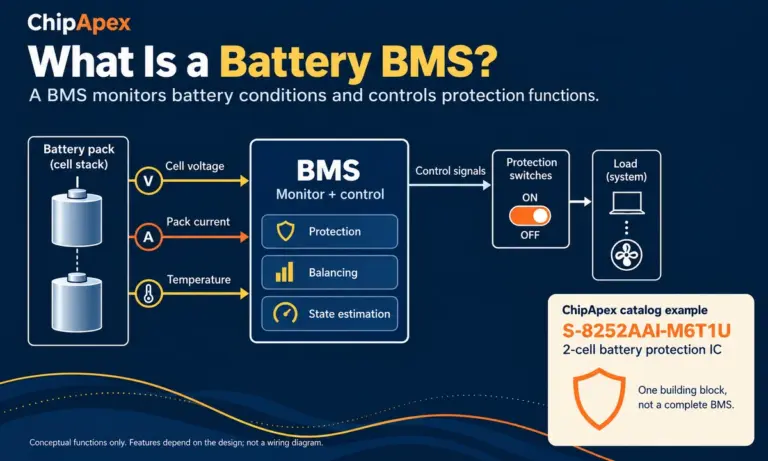
Learn what a battery BMS does, how protection differs from charging, and which pack specifications to check when sourcing BMS components through ChipApex.
Read More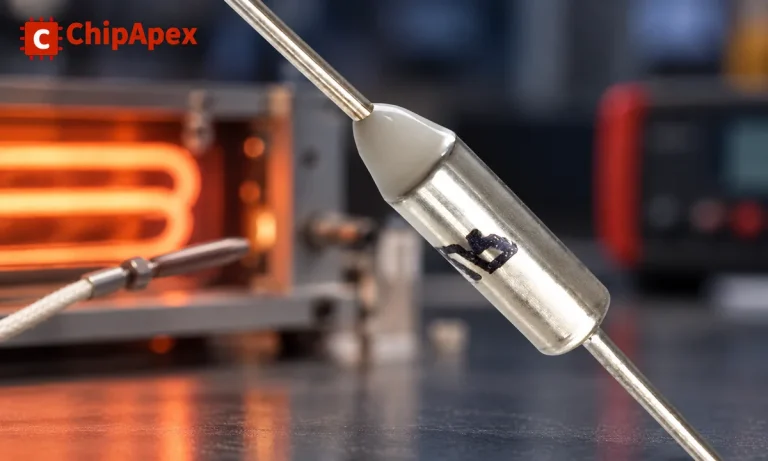
Understand thermal fuse operation, Tf, Th and Tm, electrical ratings and mounting. Check temperature limits and replacement requirements for your design.
Read More
ADG661BRU is listed in the Analog Switches, Multiplexers, Demultiplexers range at ChipApex. The manufacturer field lists Analog Devices Inc.. Its product description is IC…
Read More
ADG661BRU is listed in the Analog Switches, Multiplexers, Demultiplexers range at ChipApex. The manufacturer field lists Analog Devices Inc.. Its product description is IC…
Read More
ADG661BRU is listed in the Analog Switches, Multiplexers, Demultiplexers range at ChipApex. The manufacturer field lists Analog Devices Inc.. Its product description is IC…
Read More
The activity of extra discounts on wholesale prices is in full swing…
Please fill in your contact information and we will send you the latest wholesale price list.





