 ChipApex | Global Electronic Components Supplier

SEARCH
Search Product
Search Post
— IC芯片 | 连接器 | 传感器 | 被动器件 —
Search productSearch post
— IC芯片 | 连接器 | 传感器 | 被动器件 —
Consult the customer manager about the wholesale price.
consultation hotline:86-132-6715-2157
email:[email protected]
Contact the product manager for consultation. One-stop consultation is available.
Do you want a lower wholesale price? Please send us your inquiry and we will reply immediately.
CDCR83DBQR is listed in the Application Specific Clock/Timing range at ChipApex. The manufacturer field lists Texas Instruments. Its product description is IC DIRECT RAMBUS CLK GEN 24-QSOP. Review the specifications below when checking this part for your BOM.
The CDCR83DBQR is a Direct Rambus clock generator (DRCG) designed for Direct Rambus memory systems supporting 800-MHz data transfer rates. It synchronizes the Rambus channel clock with external system or processor clocks using an internal PLL and phase aligner. The device operates from a single 3.3-V supply, consuming approximately 120 mW at 300 MHz. It supports frequency multipliers of 4, 6, 8, and 16/3, generating BUSCLK frequencies ranging from 267 MHz to 400 MHz. Cycle-cycle jitter is less than 50 ps at 400 MHz. Packaged in a 24-pin SSOP/QSOP (DBQ), it supports industrial temperature ranges of −40°C to 85°C.
Verify the marketing status before design inclusion, as the CDCR83 family is classified as NRND (Not Recommended for New Designs). Confirm that the DBQ package variant meets mechanical constraints. Ensure compatibility with existing system clock references (REFCLK) within the 33 MHz to 100 MHz range to maintain valid BUSCLK outputs between 267 MHz and 400 MHz.
Select this component when designing Direct Rambus memory subsystems requiring precise phase alignment between the Rambus channel and system controllers. Verify that the input REFCLK frequency allows for the desired multiply ratio (4, 6, 8, or 16/3) to achieve target BUSCLK speeds. Ensure the application environment stays within the −40°C to 85°C operating temperature range and utilizes a stable 3.3-V supply.
The CDCR83 is part of Texas Instruments' Direct Rambus clock generator family, specifically engineered for high-speed memory interfaces. It replaces discrete clock generation solutions by integrating PLL, multiplier, and phase alignment functions into a single 24-pin package. The device is designed to work in conjunction with memory controllers that divide PCLK and BUSCLK frequencies to synchronize communication domains without additional latency.
Public confirmed substitute part numbers are not available in the provided documentation. The device is marked as NRND; consult Texas Instruments for current availability or legacy support options.
Explore related parts through Clock/Timing, Integrated Circuits (ICs), all product categories, ChipApex homepage.
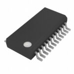 CDCR83DBQR

CDCR83DBQR is listed in the Application Specific Clock/Timing range at ChipApex. The manufacturer field lists Texas Instruments. Its product description is IC DIRECT RAMBUS…
Read More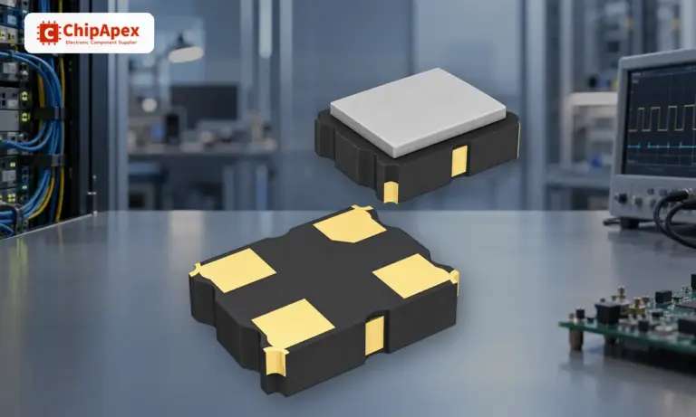
Understand how oscillators generate timing signals, how they differ from crystals, and which frequency, output and stability specs matter when choosing one.
Read More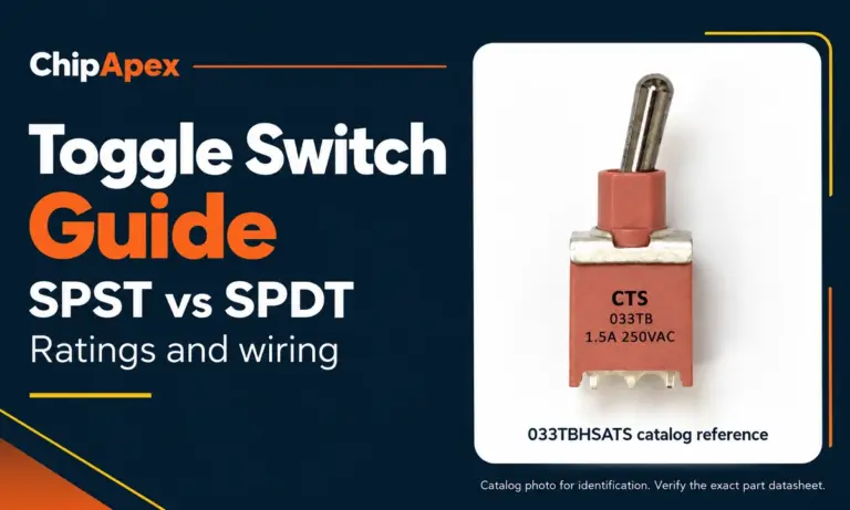
Compare SPST and SPDT toggle switches, understand AC/DC ratings, and follow wiring examples. Check contact action, mounting and parts in the ChipApex catalog.
Read More
CDCR83DBQR is listed in the Application Specific Clock/Timing range at ChipApex. The manufacturer field lists Texas Instruments. Its product description is IC DIRECT RAMBUS…
Read More
CDCR83DBQR is listed in the Application Specific Clock/Timing range at ChipApex. The manufacturer field lists Texas Instruments. Its product description is IC DIRECT RAMBUS…
Read More
CDCR83DBQR is listed in the Application Specific Clock/Timing range at ChipApex. The manufacturer field lists Texas Instruments. Its product description is IC DIRECT RAMBUS…
Read More
CDCR83DBQR is listed in the Application Specific Clock/Timing range at ChipApex. The manufacturer field lists Texas Instruments. Its product description is IC DIRECT RAMBUS…
Read More
CDCR83DBQR is listed in the Application Specific Clock/Timing range at ChipApex. The manufacturer field lists Texas Instruments. Its product description is IC DIRECT RAMBUS…
Read More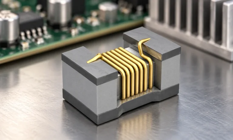
See when an inductor behaves linearly, how DC bias and saturation reduce inductance, and which current and temperature curves to check.
Read More
CDCR83DBQR is listed in the Application Specific Clock/Timing range at ChipApex. The manufacturer field lists Texas Instruments. Its product description is IC DIRECT RAMBUS…
Read More
CDCR83DBQR is listed in the Application Specific Clock/Timing range at ChipApex. The manufacturer field lists Texas Instruments. Its product description is IC DIRECT RAMBUS…
Read More
CDCR83DBQR is listed in the Application Specific Clock/Timing range at ChipApex. The manufacturer field lists Texas Instruments. Its product description is IC DIRECT RAMBUS…
Read More
The activity of extra discounts on wholesale prices is in full swing…
Please fill in your contact information and we will send you the latest wholesale price list.





