 ChipApex | Global Electronic Components Supplier

SEARCH
Search Product
Search Post
— IC芯片 | 连接器 | 传感器 | 被动器件 —
Search productSearch post
— IC芯片 | 连接器 | 传感器 | 被动器件 —
Consult the customer manager about the wholesale price.
consultation hotline:86-132-6715-2157
email:[email protected]
Contact the product manager for consultation. One-stop consultation is available.
Do you want a lower wholesale price? Please send us your inquiry and we will reply immediately.
CSSTV32852GKFREP is listed in the Specialty Logic range at ChipApex. The manufacturer field lists Texas Instruments. Its product description is IC REGISTERED BUFF 114LFBGA. Review the specifications below when checking this part for your BOM.
The CSSTV32852GKFREP is a 24-bit to 48-bit registered buffer with SSTL_2 inputs and outputs. It operates from a 2.3-V to 2.7-V VCC supply and supports LVCMOS switching levels on the RESET input. The device features differential clock (CLK and CLK) inputs and meets SSTL_2 Class II specifications. It includes an enhanced diminishing manufacturing sources support program and extended temperature performance ranging from -40 °C to 85 °C.
Verify the specific ordering suffix GKFREP corresponds to the Microstar BGA package and tape-and-reel quantity of 1000 units. Confirm the part number matches the SN74SSTV32852-EP family designation for correct electrical characteristics and pinout compatibility during procurement.
Select this component when designing systems requiring widebus registered buffering with SSTL_2 interface compatibility. Ensure the design accommodates the 2.3-V to 2.7-V supply voltage range and utilizes differential clocking. Verify that the -40 °C to 85 °C operating temperature range meets the environmental requirements of the target application.
This part belongs to the Texas Instruments Widebus family, specifically designed as a registered buffer. It is part of the SN74SSTV32852-EP series, which emphasizes controlled baseline manufacturing and enhanced diminishing manufacturing sources support. The device integrates 24 bits of data path functionality into a single package for high-density memory designs.
Direct replacements include other variants within the SN74SSTV32852-EP family such as the SN74SSTV32852DW or SN74SSTV32852DWR, provided they match the required package type and temperature grade. Verify pinout and electrical specifications before substitution.
The RESET input disables the differential input receivers, resets all registers, and forces all outputs low. It must be held at a valid logic high or low level.
Data are registered at the crossing of the differential clock signals, specifically when CLK goes high and CLK goes low.
The RESET input supports LVCMOS switching levels, requiring a high-level input voltage of at least 1.7 V and a low-level input voltage of no more than 0.7 V.
Explore related parts through Logic, Integrated Circuits (ICs), all product categories, ChipApex homepage.
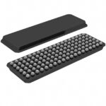 CSSTV32852GKFREP
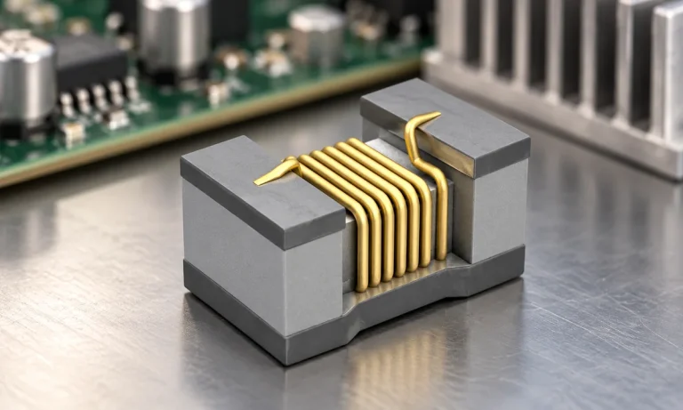
See when an inductor behaves linearly, how DC bias and saturation reduce inductance, and which current and temperature curves to check.
Read More
CSSTV32852GKFREP is listed in the Specialty Logic range at ChipApex. The manufacturer field lists Texas Instruments. Its product description is IC REGISTERED BUFF 114LFBGA.…
Read More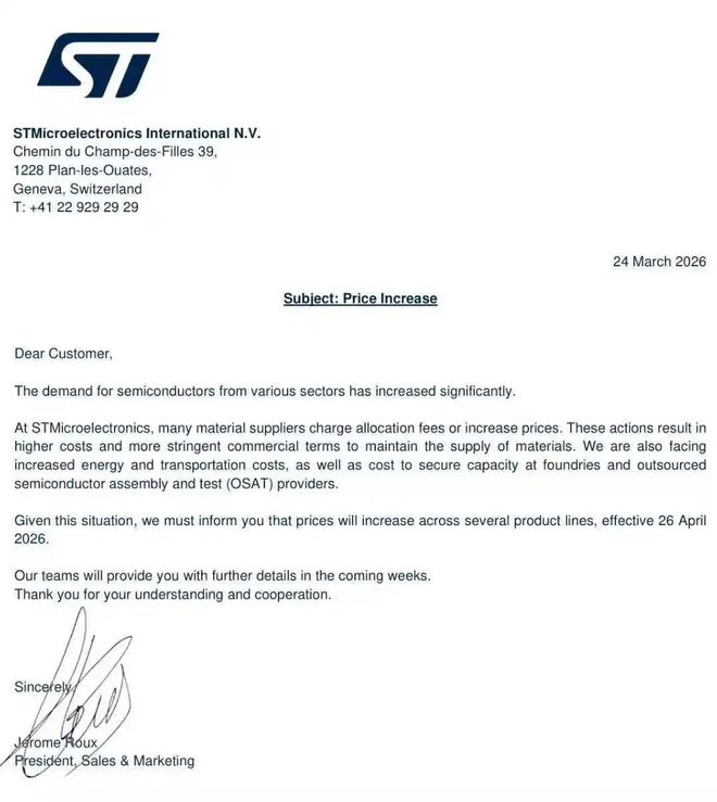
CSSTV32852GKFREP is listed in the Specialty Logic range at ChipApex. The manufacturer field lists Texas Instruments. Its product description is IC REGISTERED BUFF 114LFBGA.…
Read More
CSSTV32852GKFREP is listed in the Specialty Logic range at ChipApex. The manufacturer field lists Texas Instruments. Its product description is IC REGISTERED BUFF 114LFBGA.…
Read More
CSSTV32852GKFREP is listed in the Specialty Logic range at ChipApex. The manufacturer field lists Texas Instruments. Its product description is IC REGISTERED BUFF 114LFBGA.…
Read More
Compare Pt100 and Pt1000 RTDs, two-, three- and four-wire connections, excitation and self-heating. Build an error budget from element to reported temperature.
Read More
Choose a DIP switch by contact type, coded positions, footprint and signal ratings. Check logic polarity, assembly conditions and PCB configuration behavior.
Read More
CSSTV32852GKFREP is listed in the Specialty Logic range at ChipApex. The manufacturer field lists Texas Instruments. Its product description is IC REGISTERED BUFF 114LFBGA.…
Read More
CSSTV32852GKFREP is listed in the Specialty Logic range at ChipApex. The manufacturer field lists Texas Instruments. Its product description is IC REGISTERED BUFF 114LFBGA.…
Read More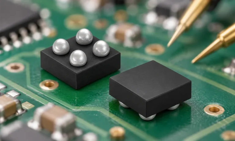
Understand how a comparator switches at a voltage threshold, why hysteresis prevents chatter, and which output and input specs matter.
Read More
CSSTV32852GKFREP is listed in the Specialty Logic range at ChipApex. The manufacturer field lists Texas Instruments. Its product description is IC REGISTERED BUFF 114LFBGA.…
Read More
CSSTV32852GKFREP is listed in the Specialty Logic range at ChipApex. The manufacturer field lists Texas Instruments. Its product description is IC REGISTERED BUFF 114LFBGA.…
Read More
The activity of extra discounts on wholesale prices is in full swing…
Please fill in your contact information and we will send you the latest wholesale price list.





