 ChipApex | Global Electronic Components Supplier

SEARCH
Search Product
Search Post
— IC芯片 | 连接器 | 传感器 | 被动器件 —
Search productSearch post
— IC芯片 | 连接器 | 传感器 | 被动器件 —
Consult the customer manager about the wholesale price.
consultation hotline:86-132-6715-2157
email:[email protected]
Contact the product manager for consultation. One-stop consultation is available.
Do you want a lower wholesale price? Please send us your inquiry and we will reply immediately.
CTSLV310QG is listed in the Clock Buffers, Drivers range at ChipApex. The manufacturer field lists CTS-Frequency Controls. Its product description is IC CLK BUFFER 1:2 1.6GHZ. Review the specifications below when checking this part for your BOM.
The CTSLV310 is a configurable ultra-low phase noise buffer and translator IC from CTS-Frequency Controls, designed for clock distribution applications. It supports LVPECL or LVDS outputs with selectable ÷1 or ÷2 division ratios and active high/low enable polarity. The device operates on a 2.375V to 3.6V supply and achieves a maximum frequency of 1.6 GHz in divide-by-two mode. Key electrical specifications include a phase noise floor of -167 dBc/Hz for LVPECL and -165 dBc/Hz for LVDS at a 1 MHz offset. Integrated jitter is specified at 26 fs for LVPECL and 36 fs for LVDS over a 12 kHz to 20 MHz bandwidth at a 155 MHz carrier. The component is available in SON8 and MSOP8 surface-mount packages.
Verify the specific package variant required for the design, as the CTSLV310 is offered in SON8 (suffix QG) and MSOP8 (suffix TG). Confirm that the configuration pins b-0 and b-1 are correctly tied to logic levels to establish the desired output type and division ratio before integration. Ensure input signal swing meets the minimum 0.2 VPP recommendation to maintain specified phase noise performance.
Select the CTSLV310 when both LVPECL and LVDS compatibility is needed within a single footprint. Choose the ÷2 mode if operating frequencies up to 1.6 GHz are required, noting that the ÷1 mode is limited to 1 GHz. Consider the MSOP8 package for standard PCB layouts or SON8 for compact designs. Verify that the application can accommodate the internal 10kΩ input bias resistor or provide appropriate AC coupling.
The CTSLV310 belongs to CTS-Frequency Controls' family of ultra-low phase noise clock buffers. It serves as a flexible solution for designers needing to translate oscillator outputs into differential formats without adding significant jitter. Unlike fixed-output buffers, its configurability reduces bill-of-materials complexity by supporting multiple interface standards through hardware pin selection.
Public confirmed substitute part numbers are not provided in the source documentation. Designers should evaluate alternative configurable LVPECL/LVDS translators based on package compatibility and phase noise specifications if this component is unavailable.
Configuration is determined by the static voltage levels on pins b-0 and b-1. Table 1 in the datasheet details the eight possible combinations for selecting LVPECL or LVDS outputs, ÷1 or ÷2 division, and enable polarity.
The maximum input frequency is 1 GHz in ÷1 mode and 1.6 GHz in ÷2 mode.
Outputs should be terminated identically using external 50Ω resistors to match LVPECL levels. Both Q and QN outputs must be terminated symmetrically to prevent waveform distortion and circulating current, even if only one output is used.
Explore related parts through Clock/Timing, Integrated Circuits (ICs), all product categories, ChipApex homepage.
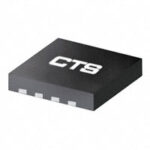 CTSLV310QG

CTSLV310QG is listed in the Clock Buffers, Drivers range at ChipApex. The manufacturer field lists CTS-Frequency Controls. Its product description is IC CLK BUFFER…
Read More
CTSLV310QG is listed in the Clock Buffers, Drivers range at ChipApex. The manufacturer field lists CTS-Frequency Controls. Its product description is IC CLK BUFFER…
Read More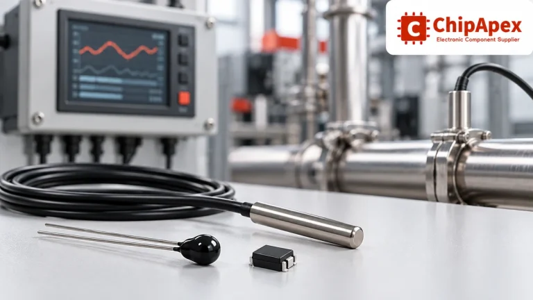
Compare thermistors, RTDs, thermocouples and temperature ICs. Learn how range, accuracy, response, interfaces and mounting affect component selection.
Read More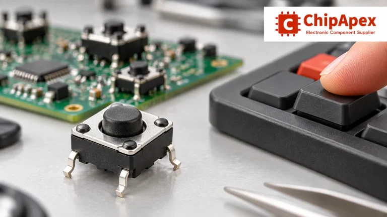
Understand tactile switches, PCB and keyboard differences, four-pin wiring, debounce, force, travel and replacement checks for reliable control inputs.
Read More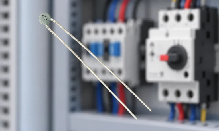
Learn why PTC resistance rises with temperature, how it differs from NTC, and which ratings matter for sensing and protection.
Read More
CTSLV310QG is listed in the Clock Buffers, Drivers range at ChipApex. The manufacturer field lists CTS-Frequency Controls. Its product description is IC CLK BUFFER…
Read More
CTSLV310QG is listed in the Clock Buffers, Drivers range at ChipApex. The manufacturer field lists CTS-Frequency Controls. Its product description is IC CLK BUFFER…
Read More
CTSLV310QG is listed in the Clock Buffers, Drivers range at ChipApex. The manufacturer field lists CTS-Frequency Controls. Its product description is IC CLK BUFFER…
Read More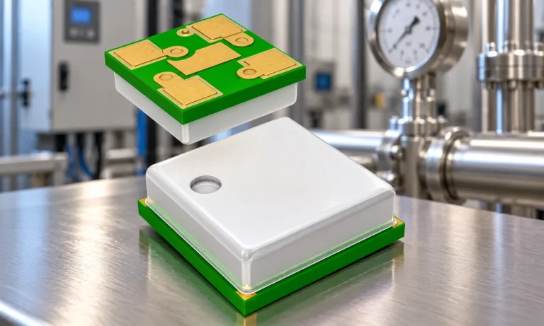
Learn how a pressure transducer converts pressure into voltage, current, or digital output, and compare pressure references and key selection specs.
Read More
CTSLV310QG is listed in the Clock Buffers, Drivers range at ChipApex. The manufacturer field lists CTS-Frequency Controls. Its product description is IC CLK BUFFER…
Read More
CTSLV310QG is listed in the Clock Buffers, Drivers range at ChipApex. The manufacturer field lists CTS-Frequency Controls. Its product description is IC CLK BUFFER…
Read More
CTSLV310QG is listed in the Clock Buffers, Drivers range at ChipApex. The manufacturer field lists CTS-Frequency Controls. Its product description is IC CLK BUFFER…
Read More
The activity of extra discounts on wholesale prices is in full swing…
Please fill in your contact information and we will send you the latest wholesale price list.





