 ChipApex | Global Electronic Components Supplier

SEARCH
Search Product
Search Post
— IC芯片 | 连接器 | 传感器 | 被动器件 —
Search productSearch post
— IC芯片 | 连接器 | 传感器 | 被动器件 —
Consult the customer manager about the wholesale price.
consultation hotline:86-132-6715-2157
email:[email protected]
Contact the product manager for consultation. One-stop consultation is available.
Do you want a lower wholesale price? Please send us your inquiry and we will reply immediately.
CY7C25682KV18-450BZC is listed in the Memory IC range at ChipApex. The manufacturer field lists Cypress Semiconductor Corp. Its product description is IC SRAM 72MBIT PAR 165FBGA. Review the specifications below when checking this part for your BOM.
The CY7C25682KV18-450BZC is a 72-Mbit DDR II+ Synchronous Pipelined SRAM organized as 4M x 18. It supports a maximum operating frequency of 450 MHz with a typical read latency of 2.5 cycles when the DOFF pin is asserted HIGH. The device utilizes a double data rate interface, transferring data at 900 MHz. It features On-Die Termination (ODT) for DQ, BWS, and clock inputs to reduce board area and simplify routing. The core voltage is 1.8 V ± 0.1 V, while I/O voltage ranges from 1.4 V to VDD.
Verify that the specific suffix '450BZC' corresponds to the 450 MHz speed grade and lead-free FBGA packaging as defined in the official Cypress/Infineon ordering guide. Confirm that the ODT range selection via the ZQ resistor matches system impedance requirements during power-up initialization. Ensure DOFF pin configuration aligns with the desired 2.5-cycle or 1-cycle latency mode.
Select this component for applications requiring pipelined synchronous memory with DDR interface capabilities. The 4M x 18 organization suits designs needing width expansion or specific data bus widths. Consider the 450 MHz speed grade if system timing allows for lower power consumption compared to higher-speed variants. Verify compatibility with HSTL I/O standards and available echo clock routing resources.
This part belongs to the CY7C25682KV18 family of 72-Mbit DDR II+ SRAMs manufactured by Cypress Semiconductor (now Infineon). It shares architectural similarities with the CY7C25702KV18 but differs in data width organization. The series is designed for high-speed parallel memory interfaces in embedded systems.
CY7C25682KV18-500BZC offers a higher 500 MHz speed grade within the same package and functional specification.
ODT range is selected during power-up initialization via the ODT pin. A LOW selects a low range following RQ/3.33, while a HIGH selects a high range following RQ/1.66.
QVLD is a valid output indicator that asserts half a cycle before valid data arrives, helping to simplify data capture in high-speed systems.
Explore related parts through Memory, Integrated Circuits (ICs), all product categories, ChipApex homepage.
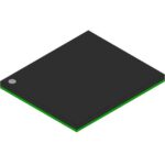 CY7C25682KV18-450BZC

CY7C25682KV18-450BZC is listed in the Memory IC range at ChipApex. The manufacturer field lists Cypress Semiconductor Corp. Its product description is IC SRAM 72MBIT…
Read More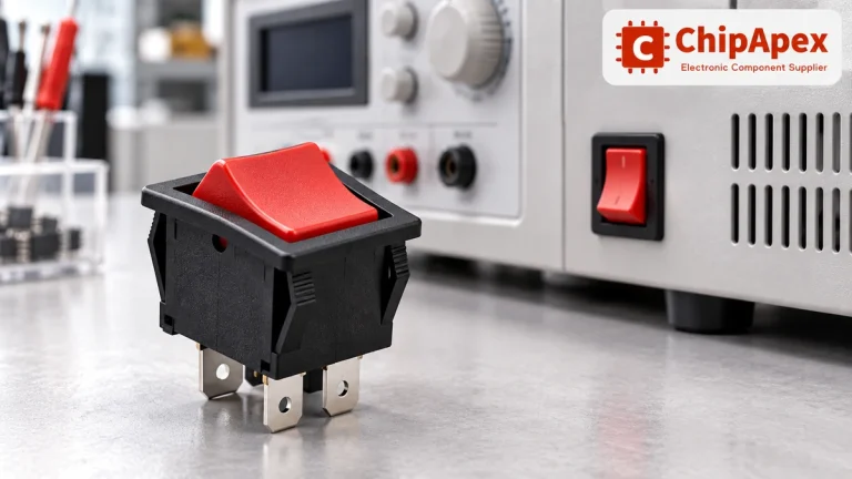
Choose a rocker switch by AC/DC ratings, contact arrangement, illumination, panel fit and sealing. Get practical checks for engineering and component sourcing.
Read More
CY7C25682KV18-450BZC is listed in the Memory IC range at ChipApex. The manufacturer field lists Cypress Semiconductor Corp. Its product description is IC SRAM 72MBIT…
Read More
CY7C25682KV18-450BZC is listed in the Memory IC range at ChipApex. The manufacturer field lists Cypress Semiconductor Corp. Its product description is IC SRAM 72MBIT…
Read More
CY7C25682KV18-450BZC is listed in the Memory IC range at ChipApex. The manufacturer field lists Cypress Semiconductor Corp. Its product description is IC SRAM 72MBIT…
Read More
CY7C25682KV18-450BZC is listed in the Memory IC range at ChipApex. The manufacturer field lists Cypress Semiconductor Corp. Its product description is IC SRAM 72MBIT…
Read More
CY7C25682KV18-450BZC is listed in the Memory IC range at ChipApex. The manufacturer field lists Cypress Semiconductor Corp. Its product description is IC SRAM 72MBIT…
Read More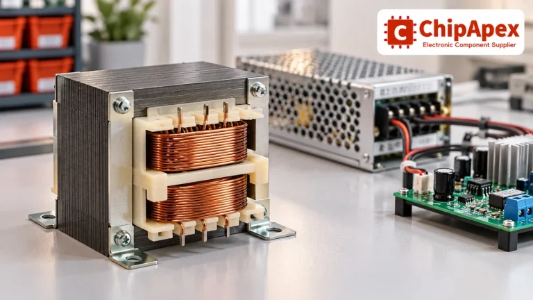
Select power transformers by input frequency, secondary VA, rectifier load, isolation, regulation and inrush. Build a clearer specification for your next RFQ.
Read More
CY7C25682KV18-450BZC is listed in the Memory IC range at ChipApex. The manufacturer field lists Cypress Semiconductor Corp. Its product description is IC SRAM 72MBIT…
Read More
CY7C25682KV18-450BZC is listed in the Memory IC range at ChipApex. The manufacturer field lists Cypress Semiconductor Corp. Its product description is IC SRAM 72MBIT…
Read More
CY7C25682KV18-450BZC is listed in the Memory IC range at ChipApex. The manufacturer field lists Cypress Semiconductor Corp. Its product description is IC SRAM 72MBIT…
Read More
CY7C25682KV18-450BZC is listed in the Memory IC range at ChipApex. The manufacturer field lists Cypress Semiconductor Corp. Its product description is IC SRAM 72MBIT…
Read More
The activity of extra discounts on wholesale prices is in full swing…
Please fill in your contact information and we will send you the latest wholesale price list.





