 ChipApex | Global Electronic Components Supplier
DG403CJ+
Search Product
Search Post
— IC芯片 | 连接器 | 传感器 | 被动器件 —
Search productSearch post
— IC芯片 | 连接器 | 传感器 | 被动器件 —
Consult the customer manager about the wholesale price.
consultation hotline:86-132-6715-2157
email:[email protected]
Contact the product manager for consultation. One-stop consultation is available.
Do you want a lower wholesale price? Please send us your inquiry and we will reply immediately.
The DG403CJ+ is a dual, high-speed analog switch in a 16-pin Plastic DIP package. It features two SPDT switches with guaranteed on-resistance matching of 2 Ω max and flatness of 3 Ω max. The device operates from single +10V to +30V or bipolar ±4.5V to ±20V supplies. Electrical characteristics include a maximum turn-on time of 150 ns, turn-off time of 100 ns, and charge injection of 15 pC max. On-resistance is 45 Ω max at TA = TMIN to TMAX. Power consumption is 35 µW max. Operating temperature range is 0°C to +70°C.
Verify the component manufacturer designation as Analog Devices Inc./Maxim Integrated. Confirm the specific suffix 'CJ+' corresponds to the 0°C to +70°C operating temperature range and 16-PDIP package. Ensure datasheet revision matches the required specifications for on-resistance and switching times before integration.
Select this part for applications requiring dual SPDT switching with tight on-resistance matching. Verify supply voltage compatibility within the +10V to +30V single or ±4.5V to ±20V bipolar ranges. Consider the 16-PDIP package constraints for PCB layout. Check if the 0°C to +70°C temperature range meets environmental requirements.
The DG403CJ+ belongs to the DG401/DG403/DG405 family of improved, dual, high-speed analog switches. These devices are fabricated using a 44V silicon-gate process. The DG403 variant specifically provides two SPDT switches, distinguishing it from the SPST DG401 and DPST DG405 configurations within the same series.
DG403DJ+
The maximum on-resistance match (ΔrDS(ON)) between channels is 2 Ω.
The maximum power consumption is 35 µW.
Yes, the device maintains TTL compatibility with VL = +5V across the specified supply range.
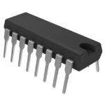 DG403CJ+
The activity of extra discounts on wholesale prices is in full swing…
Please fill in your contact information and we will send you the latest wholesale price list.





