 ChipApex | Global Electronic Components Supplier
HEF4053BTT,112
Search Product
Search Post
— IC芯片 | 连接器 | 传感器 | 被动器件 —
Search productSearch post
— IC芯片 | 连接器 | 传感器 | 被动器件 —
Consult the customer manager about the wholesale price.
consultation hotline:86-132-6715-2157
email:[email protected]
Contact the product manager for consultation. One-stop consultation is available.
Do you want a lower wholesale price? Please send us your inquiry and we will reply immediately.
The HEF4053BTT,112 is a triple single-pole double-throw (SPDT) analog switch manufactured by Nexperia USA Inc. It operates within a supply voltage range of 3.0 V to 15.0 V and supports an ambient temperature range from -40 °C to +125 °C. The device features three independent switches, each with a digital select input (Sn), two independent inputs/outputs (nY0 and nY1), and a common input/output (nZ). A shared enable input (E) controls the state of all switches simultaneously. At a 15 V supply, the typical ON resistance is 60 Ω with a maximum of 175 Ω, while the OFF-state leakage current is specified at 1000 nA. The component is housed in a TSSOP16 package (SOT403-1) with a body width of 4.4 mm.
Verify the ordering suffix '112' against official Nexperia documentation to confirm the specific tape-and-reel packaging format and quantity. Ensure the requested part matches the TSSOP16 (SOT403-1) package outline dimensions provided in the datasheet. Confirm RoHS compliance status as per the latest product data sheet revision before finalizing procurement orders.
Select this component when a triple SPDT analog switch is required for signal routing in systems operating between 3 V and 15 V. Consider the TSSOP16 package constraints regarding thermal derating above 91 °C. Evaluate the ON resistance variation across the full input voltage range and temperature spectrum to ensure signal integrity meets application requirements.
The HEF4053B series belongs to the HEF CMOS logic family designed for general-purpose switching. The HEF4053B specifically provides three independent SPDT switches sharing a common enable line. This architecture allows efficient management of multiple signal paths using minimal control pins, making it suitable for compact circuit designs requiring analog or digital signal selection.
HEF4053BT (SO16 package)
When the enable input E is HIGH, all switches are turned off regardless of the select inputs. When E is LOW, the switches operate according to the logic levels applied to their respective select inputs (Sn).
The recommended maximum input transition rise and fall rate depends on the supply voltage: 3.75 μs/V at 5 V, 0.5 μs/V at 10 V, and 0.08 μs/V at 15 V.
Yes, the inputs include clamp diodes, which enables the use of current limiting resistors to interface inputs to voltages in excess of VDD.
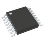 HEF4053BTT,112
The activity of extra discounts on wholesale prices is in full swing…
Please fill in your contact information and we will send you the latest wholesale price list.





