 ChipApex | Global Electronic Components Supplier
HEF4067BP,652
Search Product
Search Post
— IC芯片 | 连接器 | 传感器 | 被动器件 —
Search productSearch post
— IC芯片 | 连接器 | 传感器 | 被动器件 —
Consult the customer manager about the wholesale price.
consultation hotline:86-132-6715-2157
email:[email protected]
Contact the product manager for consultation. One-stop consultation is available.
Do you want a lower wholesale price? Please send us your inquiry and we will reply immediately.
The HEF4067BP,652 is a single-pole 16-throw analog switch manufactured by Nexperia. It functions as a 16:1 multiplexer/demultiplexer featuring four digital address inputs (A0-A3), sixteen independent I/O channels (Y0-Y15), and one common I/O pin (Z). The device operates with a supply voltage range of 3.0 V to 15.0 V. At 25 °C, the typical on-resistance is 350 Ω at 5 V, 80 Ω at 10 V, and 60 Ω at 15 V. Propagation delays range from 10 ns to 60 ns depending on voltage. It includes clamp diodes for input protection and meets ESD standards exceeding 2000 V (HBM) and 1000 V (CDM).
Verify the specific ordering suffix against the manufacturer's official documentation to confirm package type and tape/reel specifications. Ensure the component version matches the required JEDEC compliance standards. Confirm that the ambient temperature operating range aligns with the system design constraints prior to finalizing procurement orders.
Select this component when a wide supply voltage range up to 15 V is required for analog signal routing. Consider the on-resistance variation across the voltage range for signal integrity analysis. Verify that the SO24 or TSSOP24 package options fit the available PCB footprint and assembly capabilities.
The HEF4067B series belongs to the standard CMOS logic family designed for general-purpose analog switching. It serves as a foundational building block for data acquisition systems and communication equipment requiring channel selection. The device is pin-compatible with older HEF4067B variants while offering updated ESD protection characteristics.
The HEF4067BT and HEF4067BTT are direct functional equivalents within the same family, differing primarily in package style (SO24 vs TSSOP24). Cross-vendor alternatives such as the CD4067 or 74HC4067 may require verification of pinout compatibility and electrical parameter alignment.
The enable input (E) is active LOW. When E is HIGH, all switches are turned off regardless of the address inputs. When E is LOW, one switch is selected based on the A0-A3 address lines.
The recommended operating supply voltage (VDD) ranges from 3.0 V to 15.0 V. The absolute maximum rating allows up to 18 V, but operation beyond 15 V is not specified.
Yes, the inputs include clamp diodes. This allows interface to voltages in excess of VDD, provided current limiting resistors are used to protect the internal structures.
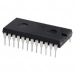 HEF4067BP,652
The activity of extra discounts on wholesale prices is in full swing…
Please fill in your contact information and we will send you the latest wholesale price list.





