 ChipApex | Global Electronic Components Supplier

SEARCH
Search Product
Search Post
— IC芯片 | 连接器 | 传感器 | 被动器件 —
Search productSearch post
— IC芯片 | 连接器 | 传感器 | 被动器件 —
Consult the customer manager about the wholesale price.
consultation hotline:86-132-6715-2157
email:[email protected]
Contact the product manager for consultation. One-stop consultation is available.
Do you want a lower wholesale price? Please send us your inquiry and we will reply immediately.
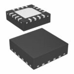
HMC744LC3TR is listed in the Clock Buffers, Drivers range at ChipApex. The manufacturer field lists Analog Devices Inc.. Its product description is IC CLK BUFFER 1:2 14GHZ 16SMD. Review the specifications below when checking this part for your BOM.
The HMC744LC3TR is a 1:2 fanout buffer designed for data transmission rates up to 14 Gbps and clock frequencies as high as 14 GHz. It features internally terminated CML inputs and source-terminated CML outputs, supporting both AC and DC coupling. The device operates from a single +3.3 V supply with typical power consumption of 287 mW. Key electrical parameters include a propagation delay of 120 ps, rise/fall times of 22/20 ps, and a programmable output voltage swing adjustable between 600 mV and 1100 mV via the VR pin. It is housed in a 16-lead ceramic SMT package.
Verify the specific ordering suffix against manufacturer documentation to confirm packaging format. The TR suffix typically indicates tape and reel packaging, while other suffixes may denote cut tape or evaluation board variants. Ensure compatibility with the required moisture sensitivity level (MSL 3) and reflow temperature limits during assembly processes.
Select this component when a high-speed 1:2 fanout buffer is required for CML signal distribution. The device is suitable for applications needing fast rise and fall times (22/20 ps) and low jitter. Consider the programmable output voltage feature if loss compensation or signal-level optimization is necessary within the design constraints.
The HMC744LC3 belongs to the HMC744 series of high-speed digital logic components manufactured by Analog Devices Inc. Originally associated with Hittite Microwave Corporation, these devices are designed for surface-mount technology (SMT) applications requiring robust performance in RF and high-speed digital environments.
Publicly confirmed substitute part numbers are not available in the provided documentation. Verify functional equivalence carefully if considering alternative components, particularly regarding CML interface compatibility and operating voltage ranges.
The output voltage swing is programmable between 600 mV and 1100 mV using the VR pin. Adjusting the voltage applied to this pin allows for signal-level optimization or loss compensation.
All differential inputs are terminated internally to 50 Ohms connected to the positive supply (Vcc). These inputs can be either AC or DC coupled.
The maximum junction temperature for the HMC744LC3 is rated at 125 °C.
Explore related parts through Clock/Timing, Integrated Circuits (ICs), all product categories, ChipApex homepage.
 HMC744LC3TR

HMC744LC3TR is listed in the Clock Buffers, Drivers range at ChipApex. The manufacturer field lists Analog Devices Inc.. Its product description is IC CLK…
Read More
HMC744LC3TR is listed in the Clock Buffers, Drivers range at ChipApex. The manufacturer field lists Analog Devices Inc.. Its product description is IC CLK…
Read More
HMC744LC3TR is listed in the Clock Buffers, Drivers range at ChipApex. The manufacturer field lists Analog Devices Inc.. Its product description is IC CLK…
Read More
HMC744LC3TR is listed in the Clock Buffers, Drivers range at ChipApex. The manufacturer field lists Analog Devices Inc.. Its product description is IC CLK…
Read More
HMC744LC3TR is listed in the Clock Buffers, Drivers range at ChipApex. The manufacturer field lists Analog Devices Inc.. Its product description is IC CLK…
Read More
HMC744LC3TR is listed in the Clock Buffers, Drivers range at ChipApex. The manufacturer field lists Analog Devices Inc.. Its product description is IC CLK…
Read More
HMC744LC3TR is listed in the Clock Buffers, Drivers range at ChipApex. The manufacturer field lists Analog Devices Inc.. Its product description is IC CLK…
Read More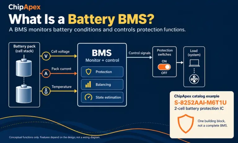
Learn what a battery BMS does, how protection differs from charging, and which pack specifications to check when sourcing BMS components through ChipApex.
Read More
HMC744LC3TR is listed in the Clock Buffers, Drivers range at ChipApex. The manufacturer field lists Analog Devices Inc.. Its product description is IC CLK…
Read More
HMC744LC3TR is listed in the Clock Buffers, Drivers range at ChipApex. The manufacturer field lists Analog Devices Inc.. Its product description is IC CLK…
Read More
HMC744LC3TR is listed in the Clock Buffers, Drivers range at ChipApex. The manufacturer field lists Analog Devices Inc.. Its product description is IC CLK…
Read More
HMC744LC3TR is listed in the Clock Buffers, Drivers range at ChipApex. The manufacturer field lists Analog Devices Inc.. Its product description is IC CLK…
Read More
The activity of extra discounts on wholesale prices is in full swing…
Please fill in your contact information and we will send you the latest wholesale price list.






