ChipApex | Global Electronic Components Supplier

SEARCH
Search Product
Search Post
— IC芯片 | 连接器 | 传感器 | 被动器件 —
Search productSearch post
— IC芯片 | 连接器 | 传感器 | 被动器件 —
Consult the customer manager about the wholesale price.
consultation hotline:86-132-6715-2157
email:[email protected]
Contact the product manager for consultation. One-stop consultation is available.
Do you want a lower wholesale price? Please send us your inquiry and we will reply immediately.
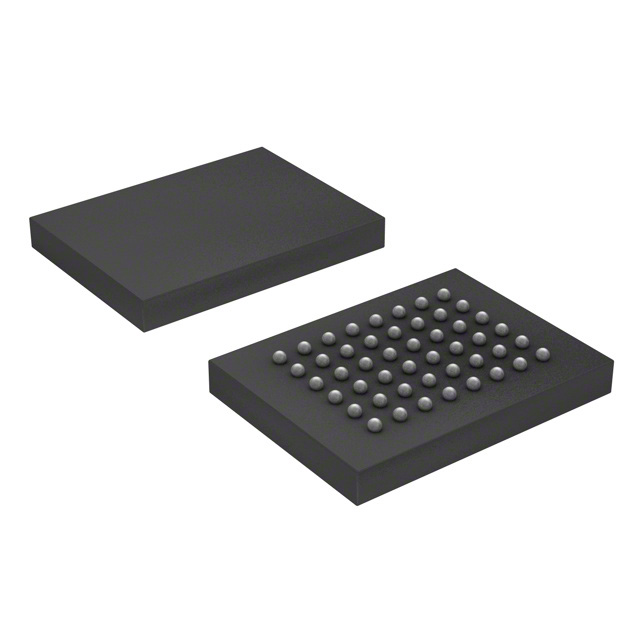
IDT71V416VL15BEGI is listed in the Memory IC range at ChipApex. The manufacturer field lists Renesas Electronics Corporation. Its product description is IC SRAM 4MBIT PARALLEL 48CABGA. Review the specifications below when checking this part for your BOM.
The IDT71V416VL15BEGI is a 4 Mbit (256K x 16) asynchronous static RAM fabricated using high-performance CMOS technology. It operates from a single 3.3V supply with access times of 15 ns and cycle times of 15 ns. The device features LVTTL-compatible bidirectional I/O, JEDEC center power/ground pinout for noise reduction, and upper/lower byte enable pins. It supports commercial (0°C to +70°C) and industrial (-40°C to +85°C) temperature ranges and is housed in a 48-ball BGA package.
Verify the specific ordering suffix against the manufacturer's datasheet to confirm the exact speed grade, package type, and temperature range. Confirm RoHS compliance status as indicated by the 'G' suffix if applicable. Ensure the component matches the required voltage and timing specifications for the target circuit design before procurement.
Select this component when a 256K x 16 organization is required with 15 ns access speeds. Consider the 48-ball BGA package for space-constrained designs requiring surface mount technology. Verify that the operating environment falls within the specified commercial or industrial temperature limits defined by the part suffix.
This component belongs to the IDT71V416 family of 4 Megabit SRAMs. The 'VL' designation indicates the low-power variant available in both commercial and industrial temperature grades. The 'BEI' suffix specifies the 48-ball BGA package and industrial temperature range, distinguishing it from SOJ or TSOP variants.
Compatible substitutes include other 256K x 16 asynchronous SRAMs with 15 ns access times and 3.3V operation. Verify pin compatibility, specifically the JEDEC center power/ground arrangement, and ensure the replacement supports the required LVTTL input/output levels and byte enable functionality.
The BHE (Byte High Enable) and BLE (Byte Low Enable) pins allow independent selection of the upper and lower bytes of the 16-bit data word for read and write operations.
Placing power and ground pins in the center of the array reduces noise coupling and improves signal integrity compared to edge-placed power pins.
Explore related parts through Memory, Integrated Circuits (ICs), all product categories, ChipApex homepage.
 IDT71V416VL15BEGI

Select a bridge rectifier by reverse voltage, capacitor charging current, startup surge and cooling. Work through a stated DC voltage and ripple example.
Read More
IDT71V416VL15BEGI is listed in the Memory IC range at ChipApex. The manufacturer field lists Renesas Electronics Corporation. Its product description is IC SRAM 4MBIT…
Read More
IDT71V416VL15BEGI is listed in the Memory IC range at ChipApex. The manufacturer field lists Renesas Electronics Corporation. Its product description is IC SRAM 4MBIT…
Read More
IDT71V416VL15BEGI is listed in the Memory IC range at ChipApex. The manufacturer field lists Renesas Electronics Corporation. Its product description is IC SRAM 4MBIT…
Read More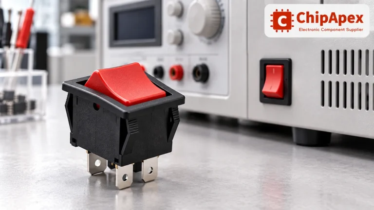
Choose a rocker switch by AC/DC ratings, contact arrangement, illumination, panel fit and sealing. Get practical checks for engineering and component sourcing.
Read More
IDT71V416VL15BEGI is listed in the Memory IC range at ChipApex. The manufacturer field lists Renesas Electronics Corporation. Its product description is IC SRAM 4MBIT…
Read More
IDT71V416VL15BEGI is listed in the Memory IC range at ChipApex. The manufacturer field lists Renesas Electronics Corporation. Its product description is IC SRAM 4MBIT…
Read More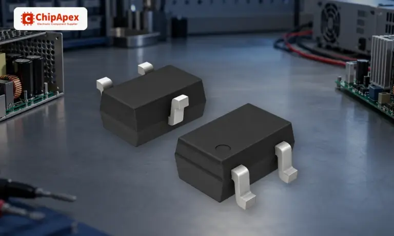
Learn how a diode conducts, how to identify anode and cathode, and when to choose rectifier, TVS, Zener or photodiode types for a circuit.
Read More
IDT71V416VL15BEGI is listed in the Memory IC range at ChipApex. The manufacturer field lists Renesas Electronics Corporation. Its product description is IC SRAM 4MBIT…
Read More
IDT71V416VL15BEGI is listed in the Memory IC range at ChipApex. The manufacturer field lists Renesas Electronics Corporation. Its product description is IC SRAM 4MBIT…
Read More
IDT71V416VL15BEGI is listed in the Memory IC range at ChipApex. The manufacturer field lists Renesas Electronics Corporation. Its product description is IC SRAM 4MBIT…
Read More
IDT71V416VL15BEGI is listed in the Memory IC range at ChipApex. The manufacturer field lists Renesas Electronics Corporation. Its product description is IC SRAM 4MBIT…
Read More
The activity of extra discounts on wholesale prices is in full swing…
Please fill in your contact information and we will send you the latest wholesale price list.