 ChipApex | Global Electronic Components Supplier

SEARCH
Search Product
Search Post
— IC芯片 | 连接器 | 传感器 | 被动器件 —
Search productSearch post
— IC芯片 | 连接器 | 传感器 | 被动器件 —
Consult the customer manager about the wholesale price.
consultation hotline:86-132-6715-2157
email:[email protected]
Contact the product manager for consultation. One-stop consultation is available.
Do you want a lower wholesale price? Please send us your inquiry and we will reply immediately.
LFXP20E-3FN484I is listed in the Field Programmable Gate Array range at ChipApex. The manufacturer field lists Lattice Semiconductor Corporation. Its product description is IC FPGA 340 I/O 484FBGA. Review the specifications below when checking this part for your BOM.
The LFXP20E-3FN484I is a non-volatile Field Programmable Gate Array from the LatticeXP family, featuring 20K logic elements and 396 Kbits of embedded block RAM. It operates at a -3 speed grade within an FPBGA-484 package, supporting up to 340 I/Os. The device utilizes ispXP technology for instant-on configuration in microseconds without external memory. It supports multiple voltage supplies including 1.2V, 1.8V, 2.5V, and 3.3V, and includes four sysCLOCK PLLs for flexible clock management.
Verify component authenticity through authorized distributors. Confirm RoHS compliance status as required by specific project regulations. Ensure proper handling procedures are followed due to moisture sensitivity classification. Validate that the -3 speed grade meets timing requirements for the target design implementation.
Select this model when non-volatile storage and instant power-up are critical requirements. The LFXP20 variant offers sufficient density for moderate complexity designs while maintaining low static power consumption. Consider the available I/O count and package constraints during initial architectural planning.
This component belongs to the LatticeXP family, which bridges the gap between CPLDs and larger FPGAs. It combines the ease of use and instant-on features of non-volatile devices with the flexibility of SRAM-based FPGAs. The family is designed for cost-sensitive applications requiring high reliability and security.
LFXP10E-3FN484I: Lower density option within the same package and speed grade. LFXP20E-6FN484I: Same density but slower speed grade. LFECP20E-3FN484I: Different architecture (SRAM-based) with similar density but requires external configuration memory.
Explore related parts through Embedded, Integrated Circuits (ICs), all product categories, ChipApex homepage.


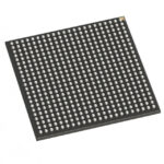 LFXP20E-3FN484I

Choose an AC to DC converter by input range, output demand, isolation, efficiency and thermal derating. Compare architectures and check installation needs.
Read More
LFXP20E-3FN484I is listed in the Field Programmable Gate Array range at ChipApex. The manufacturer field lists Lattice Semiconductor Corporation. Its product description is IC…
Read More
LFXP20E-3FN484I is listed in the Field Programmable Gate Array range at ChipApex. The manufacturer field lists Lattice Semiconductor Corporation. Its product description is IC…
Read More
LFXP20E-3FN484I is listed in the Field Programmable Gate Array range at ChipApex. The manufacturer field lists Lattice Semiconductor Corporation. Its product description is IC…
Read More
LFXP20E-3FN484I is listed in the Field Programmable Gate Array range at ChipApex. The manufacturer field lists Lattice Semiconductor Corporation. Its product description is IC…
Read More
Understand RF attenuator dB values, fixed and programmable types, impedance, power limits and noise tradeoffs before choosing parts for an RF signal path.
Read More
LFXP20E-3FN484I is listed in the Field Programmable Gate Array range at ChipApex. The manufacturer field lists Lattice Semiconductor Corporation. Its product description is IC…
Read More
LFXP20E-3FN484I is listed in the Field Programmable Gate Array range at ChipApex. The manufacturer field lists Lattice Semiconductor Corporation. Its product description is IC…
Read More
LFXP20E-3FN484I is listed in the Field Programmable Gate Array range at ChipApex. The manufacturer field lists Lattice Semiconductor Corporation. Its product description is IC…
Read More
LFXP20E-3FN484I is listed in the Field Programmable Gate Array range at ChipApex. The manufacturer field lists Lattice Semiconductor Corporation. Its product description is IC…
Read More
Learn why PTC resistance rises with temperature, how it differs from NTC, and which ratings matter for sensing and protection.
Read More
LFXP20E-3FN484I is listed in the Field Programmable Gate Array range at ChipApex. The manufacturer field lists Lattice Semiconductor Corporation. Its product description is IC…
Read More
The activity of extra discounts on wholesale prices is in full swing…
Please fill in your contact information and we will send you the latest wholesale price list.



