 ChipApex | Global Electronic Components Supplier

SEARCH
Search Product
Search Post
— IC芯片 | 连接器 | 传感器 | 被动器件 —
Search productSearch post
— IC芯片 | 连接器 | 传感器 | 被动器件 —
Consult the customer manager about the wholesale price.
consultation hotline:86-132-6715-2157
email:[email protected]
Contact the product manager for consultation. One-stop consultation is available.
Do you want a lower wholesale price? Please send us your inquiry and we will reply immediately.
LTC2151IUJ-12#TRPBF is listed in the Analog To Digital Converters (ADC) range at ChipApex. The manufacturer field lists Analog Devices Inc.. Its product description is IC ADC 12BIT PIPELINED 40QFN. Review the specifications below when checking this part for your BOM.
The LTC2151IUJ-12#TRPBF is a single-channel, 12-bit analog-to-digital converter (ADC) operating at a maximum sampling rate of 210 Msps. It features a 1.25 GHz full-power bandwidth sample-and-hold circuit and accepts a 1.5 V peak-to-peak differential input signal. The device utilizes double-data rate (DDR) LVDS digital outputs with a pipeline latency of six clock cycles. Powered by a single 1.8 V supply, it dissipates 333 mW at full speed. Key performance metrics include a typical Signal-to-Noise Ratio (SNR) of 68.5 dB and a Spurious Free Dynamic Range (SFDR) of 90 dB. The component is housed in a 40-lead, 6 mm × 6 mm QFN package.
Verify the specific suffix #TRPBF indicates tape and reel packaging when sourcing. Confirm the 'I' designation corresponds to the industrial temperature range of –40°C to 85°C. Ensure the source document matches the manufacturer's official datasheet for the LTC2151-12 family to validate pin compatibility and electrical specifications.
Select this model over the LTC2152-12 if a 210 Msps sampling rate is sufficient, as it offers lower power dissipation (333 mW vs 347 mW). Choose the 'I' grade version for operations requiring temperatures below 0°C. Ensure the application supports DDR LVDS signaling or includes appropriate level shifting if interfacing with non-LVDS logic.
This component belongs to the LTC215x-12 family, which also includes the higher-speed LTC2152-12 (250 Msps) and the lower-speed LTC2150-12 (170 Msps). All variants share identical pinouts, package types, and functional blocks, differing primarily in sampling frequency and associated power consumption profiles.
LTC2152IUJ-12#TRPBF: Higher speed (250 Msps), slightly higher power (347 mW). Pin-compatible replacement.
The input range is set via the SENSE pin. Connecting SENSE to VDD selects the internal reference and a ±0.75V range. Applying an external reference between 1.2V and 1.3V to SENSE sets the range to ±0.6 • VSENSE.
The CLKOUT+ and CLKOUT– pins provide a data output clock signal. Digital outputs transition relative to these edges, and their phase can be adjusted via the serial interface registers.
While the encode inputs (ENC+, ENC–) are designed for differential driving for optimal performance, the datasheet notes they can accept PECL, LVDS, TTL, or CMOS inputs, implying flexibility in drive schemes.
Explore related parts through Data Acquisition, Integrated Circuits (ICs), all product categories, ChipApex homepage.
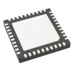 LTC2151IUJ-12#TRPBF
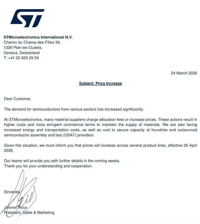
LTC2151IUJ-12#TRPBF is listed in the Analog To Digital Converters (ADC) range at ChipApex. The manufacturer field lists Analog Devices Inc.. Its product description is…
Read More
LTC2151IUJ-12#TRPBF is listed in the Analog To Digital Converters (ADC) range at ChipApex. The manufacturer field lists Analog Devices Inc.. Its product description is…
Read More
LTC2151IUJ-12#TRPBF is listed in the Analog To Digital Converters (ADC) range at ChipApex. The manufacturer field lists Analog Devices Inc.. Its product description is…
Read More
LTC2151IUJ-12#TRPBF is listed in the Analog To Digital Converters (ADC) range at ChipApex. The manufacturer field lists Analog Devices Inc.. Its product description is…
Read More
LTC2151IUJ-12#TRPBF is listed in the Analog To Digital Converters (ADC) range at ChipApex. The manufacturer field lists Analog Devices Inc.. Its product description is…
Read More
LTC2151IUJ-12#TRPBF is listed in the Analog To Digital Converters (ADC) range at ChipApex. The manufacturer field lists Analog Devices Inc.. Its product description is…
Read More
LTC2151IUJ-12#TRPBF is listed in the Analog To Digital Converters (ADC) range at ChipApex. The manufacturer field lists Analog Devices Inc.. Its product description is…
Read More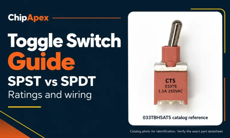
Compare SPST and SPDT toggle switches, understand AC/DC ratings, and follow wiring examples. Check contact action, mounting and parts in the ChipApex catalog.
Read More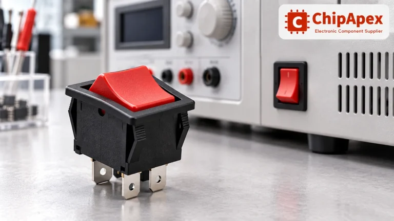
Choose a rocker switch by AC/DC ratings, contact arrangement, illumination, panel fit and sealing. Get practical checks for engineering and component sourcing.
Read More
LTC2151IUJ-12#TRPBF is listed in the Analog To Digital Converters (ADC) range at ChipApex. The manufacturer field lists Analog Devices Inc.. Its product description is…
Read More
LTC2151IUJ-12#TRPBF is listed in the Analog To Digital Converters (ADC) range at ChipApex. The manufacturer field lists Analog Devices Inc.. Its product description is…
Read More
LTC2151IUJ-12#TRPBF is listed in the Analog To Digital Converters (ADC) range at ChipApex. The manufacturer field lists Analog Devices Inc.. Its product description is…
Read More
The activity of extra discounts on wholesale prices is in full swing…
Please fill in your contact information and we will send you the latest wholesale price list.




