ChipApex | Global Electronic Components Supplier

SEARCH
Search Product
Search Post
— IC芯片 | 连接器 | 传感器 | 被动器件 —
Search productSearch post
— IC芯片 | 连接器 | 传感器 | 被动器件 —
Consult the customer manager about the wholesale price.
consultation hotline:86-132-6715-2157
email:[email protected]
Contact the product manager for consultation. One-stop consultation is available.
Do you want a lower wholesale price? Please send us your inquiry and we will reply immediately.
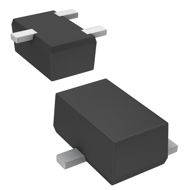
MA3J142D0L is listed in the Diode Arrays range at ChipApex. The manufacturer field lists Panasonic Electronic Components. Its product description is DIODE ARRAY GP 80V 100MA SMINI3. Review the specifications below when checking this part for your BOM.
The MA3J142D0L is a silicon epitaxial planar switching diode manufactured by Panasonic Electronic Components. It contains two isolated elements within a single SMini3-F1 package, designed for high-density mounting in switching circuits. The device features an 80 V reverse voltage rating and supports a maximum peak forward current of 225 mA per element. Electrical characteristics include a forward voltage of 1.2 V at 100 mA, a reverse current of 100 nA at 75 V, and a terminal capacitance of 15 pF. The reverse recovery time is specified at 10 ns.
Verify the specific ordering suffix against official Panasonic documentation before procurement. Confirm that the component lifecycle status aligns with long-term production requirements. Ensure the selected package variant matches the intended PCB footprint. Cross-reference absolute maximum ratings with system operating conditions to prevent overstress during transient events.
Select this component when dual isolated switching functions are required in a minimal footprint. Evaluate the 10 ns reverse recovery time against signal frequencies to ensure adequate performance. Verify thermal management capabilities relative to the junction temperature limits under continuous load conditions.
This part belongs to the MA3J142 series of silicon epitaxial planar diodes from Panasonic. The series includes variants such as the MA3J142E, which shares similar packaging but may differ in specific electrical parameters. These components are classified as general-purpose switching diodes suitable for standard industrial and consumer electronics.
Consult official manufacturer substitution lists for verified equivalents. Generic cross-references should be validated against pinout compatibility and electrical specifications prior to implementation.
The device contains two isolated elements. Pin 1 serves as the cathode for the first element, Pin 2 is the cathode for the second element, and Pin 3 acts as the common anode.
While both share the same package and general structure, they are distinguished by their marking symbols (MO for D, MU for E) and potentially specific reverse recovery time variations defined in the datasheet.
The maximum non-repetitive peak forward surge current is 500 mA for a single element and 750 mA for double operation.
Explore related parts through Rectifiers, Diodes, Discrete Semiconductor Products, all product categories.
 MA3J142D0L
Understand how a comparator switches at a voltage threshold, why hysteresis prevents chatter, and which output and input specs matter.
Read More
Learn what an IMU measures, how accelerometers and gyroscopes work together, why orientation estimates drift, and what to compare.
Read More
MA3J142D0L is listed in the Diode Arrays range at ChipApex. The manufacturer field lists Panasonic Electronic Components. Its product description is DIODE ARRAY GP…
Read More
MA3J142D0L is listed in the Diode Arrays range at ChipApex. The manufacturer field lists Panasonic Electronic Components. Its product description is DIODE ARRAY GP…
Read More
MA3J142D0L is listed in the Diode Arrays range at ChipApex. The manufacturer field lists Panasonic Electronic Components. Its product description is DIODE ARRAY GP…
Read More
MA3J142D0L is listed in the Diode Arrays range at ChipApex. The manufacturer field lists Panasonic Electronic Components. Its product description is DIODE ARRAY GP…
Read More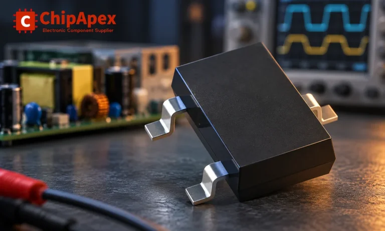
Learn how rectifiers convert AC to DC, compare half-wave and bridge circuits, and select voltage, current, recovery and thermal ratings for your design.
Read More
MA3J142D0L is listed in the Diode Arrays range at ChipApex. The manufacturer field lists Panasonic Electronic Components. Its product description is DIODE ARRAY GP…
Read More
MA3J142D0L is listed in the Diode Arrays range at ChipApex. The manufacturer field lists Panasonic Electronic Components. Its product description is DIODE ARRAY GP…
Read More
MA3J142D0L is listed in the Diode Arrays range at ChipApex. The manufacturer field lists Panasonic Electronic Components. Its product description is DIODE ARRAY GP…
Read More
Select MOV varistors by continuous voltage, clamping behavior, surge waveform and repetition. Check thermal disconnection, fuse coordination and replacements.
Read More
MA3J142D0L is listed in the Diode Arrays range at ChipApex. The manufacturer field lists Panasonic Electronic Components. Its product description is DIODE ARRAY GP…
Read More
The activity of extra discounts on wholesale prices is in full swing…
Please fill in your contact information and we will send you the latest wholesale price list.