 ChipApex | Global Electronic Components Supplier

SEARCH
Search Product
Search Post
— IC芯片 | 连接器 | 传感器 | 被动器件 —
Search productSearch post
— IC芯片 | 连接器 | 传感器 | 被动器件 —
Consult the customer manager about the wholesale price.
consultation hotline:86-132-6715-2157
email:[email protected]
Contact the product manager for consultation. One-stop consultation is available.
Do you want a lower wholesale price? Please send us your inquiry and we will reply immediately.
NPIC6C596PW,118 is listed in the Shift Registers range at ChipApex. The manufacturer field lists Nexperia USA Inc.. Its product description is IC SHIFT REGISTER 8BIT 16TSSOP. Review the specifications below when checking this part for your BOM.
The NPIC6C596PW,118 is an 8-bit serial-in/serial or parallel-out shift register with open-drain outputs. It features separate clocks for the shift and storage registers, a serial input (DS), and a serial output (Q7S) for cascading. The device includes an asynchronous reset (MR) and an output enable (OE) input. The open-drain outputs are 33 V/100 mA continuous current extended-drain NMOS transistors designed for moderate load power applications like LEDs. Integrated voltage clamps protect against inductive transients.
Verify the specific ordering suffix ',118' against the manufacturer's official documentation to confirm packaging details and availability status. Confirm that the TSSOP16 package variant matches the design requirements. Check for any product change notices or end-of-life announcements associated with this specific part number before finalizing procurement plans.
Select this component for designs requiring high-current open-drain outputs driven by a serial interface. Ensure the supply voltage range of 4.5 V to 5.5 V aligns with the system power rails. Verify that the operating temperature range of -40 °C to +125 °C meets environmental constraints. Consider the low RDSon characteristics for efficient power handling in LED or relay driver applications.
The NPIC6C596 belongs to Nexperia's Power Logic family, specifically designed as an 8-bit shift register with integrated power outputs. It combines standard logic shifting capabilities with robust power switching features, making it suitable for direct driving of loads without additional buffer components. The TSSOP16 package offers a compact solution for space-constrained PCB layouts.
Check for alternative packages within the same NPIC6C596 family, such as SO16 or DHVQFN16, if pin compatibility allows. Verify functional equivalence with other 8-bit shift registers featuring open-drain outputs if the specific NPIC6C596 is unavailable.
The serial output Q7S is clocked out on the falling edge of SHCP, providing additional hold time in cascaded applications to ensure reliable data transfer between multiple stages.
The Output Enable (OE) input controls the state of the open-drain outputs. A LOW on OE allows the storage register data to drive the outputs, while a HIGH causes the outputs to assume a high-impedance OFF-state without affecting the register states.
Explore related parts through Logic, Integrated Circuits (ICs), all product categories, ChipApex homepage.
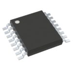 NPIC6C596PW,118

NPIC6C596PW,118 is listed in the Shift Registers range at ChipApex. The manufacturer field lists Nexperia USA Inc.. Its product description is IC SHIFT REGISTER…
Read More
NPIC6C596PW,118 is listed in the Shift Registers range at ChipApex. The manufacturer field lists Nexperia USA Inc.. Its product description is IC SHIFT REGISTER…
Read More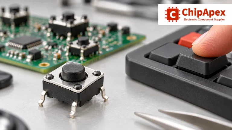
Understand tactile switches, PCB and keyboard differences, four-pin wiring, debounce, force, travel and replacement checks for reliable control inputs.
Read More
NPIC6C596PW,118 is listed in the Shift Registers range at ChipApex. The manufacturer field lists Nexperia USA Inc.. Its product description is IC SHIFT REGISTER…
Read More
NPIC6C596PW,118 is listed in the Shift Registers range at ChipApex. The manufacturer field lists Nexperia USA Inc.. Its product description is IC SHIFT REGISTER…
Read More
NPIC6C596PW,118 is listed in the Shift Registers range at ChipApex. The manufacturer field lists Nexperia USA Inc.. Its product description is IC SHIFT REGISTER…
Read More
NPIC6C596PW,118 is listed in the Shift Registers range at ChipApex. The manufacturer field lists Nexperia USA Inc.. Its product description is IC SHIFT REGISTER…
Read More
NPIC6C596PW,118 is listed in the Shift Registers range at ChipApex. The manufacturer field lists Nexperia USA Inc.. Its product description is IC SHIFT REGISTER…
Read More
Learn what an IMU measures, how accelerometers and gyroscopes work together, why orientation estimates drift, and what to compare.
Read More
NPIC6C596PW,118 is listed in the Shift Registers range at ChipApex. The manufacturer field lists Nexperia USA Inc.. Its product description is IC SHIFT REGISTER…
Read More
NPIC6C596PW,118 is listed in the Shift Registers range at ChipApex. The manufacturer field lists Nexperia USA Inc.. Its product description is IC SHIFT REGISTER…
Read More
NPIC6C596PW,118 is listed in the Shift Registers range at ChipApex. The manufacturer field lists Nexperia USA Inc.. Its product description is IC SHIFT REGISTER…
Read More
The activity of extra discounts on wholesale prices is in full swing…
Please fill in your contact information and we will send you the latest wholesale price list.






