 ChipApex | Global Electronic Components Supplier

SEARCH
Search Product
Search Post
— IC芯片 | 连接器 | 传感器 | 被动器件 —
Search productSearch post
— IC芯片 | 连接器 | 传感器 | 被动器件 —
Consult the customer manager about the wholesale price.
consultation hotline:86-132-6715-2157
email:[email protected]
Contact the product manager for consultation. One-stop consultation is available.
Do you want a lower wholesale price? Please send us your inquiry and we will reply immediately.
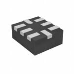
NTSX2102GU8X is listed in the Translators, Level Shifters range at ChipApex. The manufacturer field lists NXP USA Inc.. Its product description is IC TRANSLTR BIDIRECTIONAL 8XQFN. Review the specifications below when checking this part for your BOM.
The NTSX2102GU8X is a dual-supply translating transceiver with auto direction sensing, designed for bidirectional voltage level translation. It features two 2-bit input-output ports (An and Bn) and one output enable input (OE). Both supply pins, VCC(A) and VCC(B), operate within a range of 1.65 V to 5.5 V, supporting translation between standard voltage nodes such as 1.8 V, 2.5 V, 3.3 V, and 5.0 V. The device includes IOFF circuitry for partial power-down applications, preventing backflow current when powered down. It supports maximum data rates up to 50 Mbps and operates from -40 °C to +85 °C.
Verify the specific ordering suffix 'X' against official documentation to confirm tape-and-reel packaging status, as datasheet tables list 'NTSX2102GU8' without the suffix. Confirm RoHS compliance and REACH SVHC declarations via the manufacturer's Certificate of Analysis. Ensure the package type matches the XQFN8 SOT1309-1 outline specifications.
Select this component for designs requiring flexible voltage translation between 1.65 V and 5.5 V domains. The open-drain output structure necessitates external pull-up resistors on both A and B ports. Consider the 600 pF maximum capacitive load limit and ensure PCB trace lengths minimize reflections to avoid one-shot retriggering during high-speed transitions.
The NTSX2102 series comprises dual-supply translating transceivers available in multiple packages including XQFN8, XSON8, and TSSOP8. The GU8 variant specifically denotes the XQFN8 package (SOT1309-1). This family targets point-to-point applications where devices operate at different supply voltages, offering a compact solution for system integration without complex control logic.
NTSX2102GU8H
The integrated IOFF circuitry disables outputs when either VCC(A) or VCC(B) is at GND level, preventing damaging backflow current through the device.
The maximum data rate is dependent on the output impedance and edge-rate of the external open-drain driver, as well as the capacitive loading on the lines.
Explore related parts through Logic, Integrated Circuits (ICs), all product categories, ChipApex homepage.
 NTSX2102GU8X

NTSX2102GU8X is listed in the Translators, Level Shifters range at ChipApex. The manufacturer field lists NXP USA Inc.. Its product description is IC TRANSLTR…
Read More
Find out when a bare shock switch needs a pull resistor, when an MCU internal pull-up is enough, and why sensor modules and piezo…
Read More
Learn the relay definition, coil and contact operation, NO and NC forms, load ratings and suppression choices. Compare mechanical, reed and solid-state types.
Read More
NTSX2102GU8X is listed in the Translators, Level Shifters range at ChipApex. The manufacturer field lists NXP USA Inc.. Its product description is IC TRANSLTR…
Read More
Compare thermistors, RTDs, thermocouples and temperature ICs. Learn how range, accuracy, response, interfaces and mounting affect component selection.
Read More
NTSX2102GU8X is listed in the Translators, Level Shifters range at ChipApex. The manufacturer field lists NXP USA Inc.. Its product description is IC TRANSLTR…
Read More
NTSX2102GU8X is listed in the Translators, Level Shifters range at ChipApex. The manufacturer field lists NXP USA Inc.. Its product description is IC TRANSLTR…
Read More
NTSX2102GU8X is listed in the Translators, Level Shifters range at ChipApex. The manufacturer field lists NXP USA Inc.. Its product description is IC TRANSLTR…
Read More
See when an inductor behaves linearly, how DC bias and saturation reduce inductance, and which current and temperature curves to check.
Read More
NTSX2102GU8X is listed in the Translators, Level Shifters range at ChipApex. The manufacturer field lists NXP USA Inc.. Its product description is IC TRANSLTR…
Read More
NTSX2102GU8X is listed in the Translators, Level Shifters range at ChipApex. The manufacturer field lists NXP USA Inc.. Its product description is IC TRANSLTR…
Read More
NTSX2102GU8X is listed in the Translators, Level Shifters range at ChipApex. The manufacturer field lists NXP USA Inc.. Its product description is IC TRANSLTR…
Read More
The activity of extra discounts on wholesale prices is in full swing…
Please fill in your contact information and we will send you the latest wholesale price list.





